Legacy-Free Keyboard/Embedded Controller with SPI and LPC Docking Interface
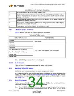
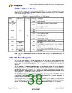
Table 3.2 Basic LPC Bus Cycle Description
1
2
A cycle is started by the host by driving LFRAME# active.
The host puts appropriate information related to the cycle on the LAD[3:0] signal lines such as
address. For target cycles, the host also drives cycle type (memory or I/O), read/write direction,
and size of the transfer.
3
4
5
The host optionally drives the data on the LAD[3:0] pins and turns the bus around to monitor the
peripheral for completion of the cycle.
The peripheral indicates completion of the cycle by driving appropriate values on the LAD[3:0]
signal lines, and potentially drives data.
The peripheral turns the bus around to the host, ending the cycle.
3.1.2
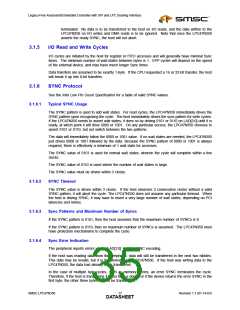
LPC Bus Cycles Summary
Table 3.3 illustrates cycle types are supported by the LPC Bus protocol.
Table 3.3 LPC Bus Cycles
CYCLE TYPE (See Note)
TRANSFER SIZE
I/O Write
I/O Read
DMA Write
1 Byte Transfer
DMA Read
Bus Master Write (I/O and Memory)
Bus Master Read (I/O and Memory)
Memory Read
1, 2, or 4 bytes - Not supported in the LPC47N350
Memory Write
Note: LPC47N350 ignores cycles that it does not support.
32-Bit Transfers
3.1.2.1
The LPC47N350 LPC Bus implementation does not support 32-bit transfers.
3.1.3
Standard LFRAME# Usage
See the Intel Low Pin Count Specification for general description of LFRAME#.
All LPC bus cycles start the same way: the chipset asserts LFRAME# for one or more clocks and drives
a START value on the LAD[3:0] pins (see Section 3.1.7, "I/O Start Fields," on page 18). Upon observing
LFRAME# active, the peripheral must stop driving the LAD[3:0] signals, even if in the middle of a transfer
(see Section 3.1.4).
3.1.4
Abort Mechanism
The host can use LFRAME# to force the LPC47N350 off the LPC Bus. See the Intel Low Pin Count
Specification for timing for the abort mechanism using LFRAME#.
Note: The LPC47N350 adheres to the following abort policy: on target I/O cycles, if the host signals
an abort before the peripheral has asserted the ‘ready’ or ‘error’ SYNC, the cycle will be
Revision 1.1 (01-14-03)
SMSC LPC47N350
DATA1S6HEET

 SMSC [ SMSC CORPORATION ]