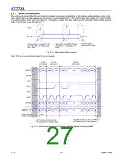
ST7735
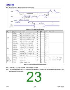
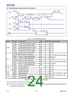
8.2 Serial interface characteristics (3-line serial)
VIH
CSX
VIL
TCHW
TSCYCW/TSCYCR
TSLW/TSLR
TCSH
TCSS
TSCC
VIH
SCL
SDA
VIL
TSHW/TSHR
TSDS
TSDH
VIH
VIL
VIH
VIL
TACC
TOH
VIH
VIL
SDA
(DOUT)
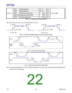
Fig. 8.2.1 3-line serial interface timing
Signal
Symbol
TCSS
TCSH
TCSS
TSCC
TCHW
Parameter
Min
15
15
60
65
40
66
30
30
150
60
60
10
10
10
Max
Unit
ns
ns
ns
ns
ns
ns
ns
ns
ns
ns
ns
ns
ns
ns
ns
Description
Chip select setup time (write)
Chip select hold time (write)
Chip select setup time (read)
Chip select hold time (read)
Chip select “H” pulse width
CSX
TSCYCW Serial clock cycle (Write)
TSHW
TSLW
SCL “H” pulse width (Write)
SCL “L” pulse width (Write)
SCL
TSCYCR Serial clock cycle (Read)
TSHR
TSLR
TSDS
TSDH
TACC
TOH
SCL “H” pulse width (Read)
SCL “L” pulse width (Read)
Data setup time
SDA
Data hold time
For maximum CL=30pF
For minimum CL=8pF
(DIN)
Access time
50
50
(DOUT)
Output disable time
Table 8.2.1 3-line Serial Interface Characteristics
Note 1: VDDI=1.65 to 3.3V, VDD=2.6 to 3.3V, AGND=DGND=0V, Ta=25
℃
Note 2: The rising time and falling time (Tr, Tf) of input signal are specified at 15 ns or less. Logic high and low levels are specified as 30%
and 70% of VDDI for Input signals.
V1.7
23
2009-12-04

 SITRONIX [ SITRONIX TECHNOLOGY CO., LTD. ]