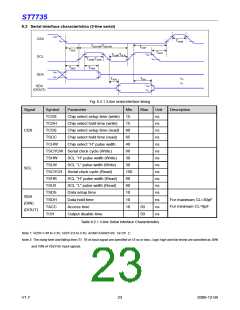
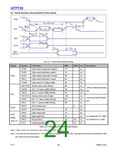
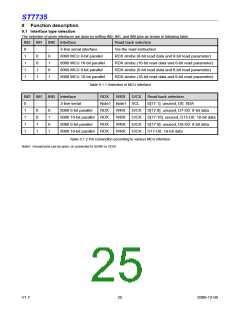
ST7735
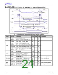
TDST
Data setup time
10
10
ns
ns
ns
ns
ns
TDHT
TRAT
Data hold time
D[17:0]
For CL=30pF
Read access time (ID)
40
40
80
TRATFM Read access time (FM)
TODH Output disable time
Table 8.1.1 Parallel Interface Characteristics
Note: VDDI=1.65 to 3.3V, VDD=2.6 to 3.3V, AGND=DGND=0V, Ta=25
℃
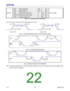
TR
TF
TR
TF
VIH=0.7 x VDDI
VIL=0.3 x VDDI
TR=TF<=15ns
VOH=0.8 x VDDI
VOL=0.2 x VDDI
TR=TF<=15ns
Fig. 8.1.2 Rising and falling timing for input and output signal
Fig. 8.1.3 Chip selection (CSX) timing
Fig. 8.1.4 Write-to-read and read-to-write timing
Note: The rising time and falling time (Tr, Tf) of input signal are specified at 15 ns or less. Logic high and low levels are specified as 30%
and 70% of VDDI for Input signals.
V1.7
22
2009-12-04

 SITRONIX [ SITRONIX TECHNOLOGY CO., LTD. ]