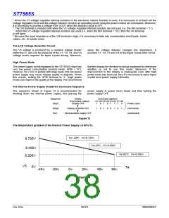
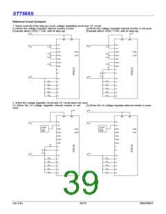
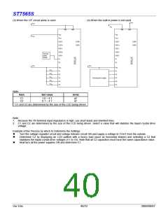
ST7565S
The Reset Circuit
When the /RES input comes to the “L” level, these LSIs return
to the default state. Their default states are as follows:
1. Display OFF
18. Electronic volume register set mode clear Electronic
volume register :
(D5, D4, D3, D2, D1, D0) = (1, 0. 0, 0, 0,0)
2. Normal display
19. Test mode clear
3. ADC select: Normal (ADC command D0 = “L”)
4. Power control register: (D2, D1, D0) = (0, 0, 0)
5. Serial interface internal register data clear
6. LCD power supply bias rate:
On the other hand, when the reset command is used, the
above default settings from 11 to 19 are only executed.
When the power is turned on, the IC internal state becomes
unstable, and it is necessary to initialize it using the /RES
terminal. After the initialization, each input terminal should
be controlled normally.
1/65 DUTY = 1/9 bias
1/49,1/55,1/53 DUTY = 1/8 bias
1/33 DUTY = 1/6 bias
7. All-indicator lamps-on OFF
(All-indicator lamps ON/OFF command D0 = “L”)
8. Power saving clear
9. V5 voltage regulator internal resistors Ra and Rb
separation
10. Output conditions of SEG and COM terminals
SEG=VDD , COM=VDD
11. Read modify write OFF
12. Static indicator OFF Static indicator register : (D1, D2) =
(0, 0)
Moreover, when the control signal from the MPU is in the high
impedance, an over current may flow to the IC. After applying
a current, it is necessary to take proper measures to prevent
the input terminal from getting into the high impedance state.
If the internal liquid crystal power supply circuit is not used on
ST7565S,it is necessary that /RES is “H” when the external
liquid crystal power supply is turned on. This IC has the
function to discharge V5 when /RES is “L,” and the external
power supply short-circuits to VDD when /RES is “L”. This
means that an internal resistor is connected between VDD
and V5.
13. Display start line set to first line
14. Column address set to Address 0
15. Page address set to Page 0
16. Common output status normal
17. V5 voltage regulator internal resistor ratio set mode clear
While /RES is “L,” the oscillator works but the display timing
generator stops, and the CL, FR, FRS and /DOF terminals
are fixed to “H.” The terminals D0 to D7 are not affected. The
VDD level is output from the SEG and COM output terminals
after a successful hardware reset.
Ver 0.6c
41/72
2009/09/07

 SITRONIX [ SITRONIX TECHNOLOGY CO., LTD. ]