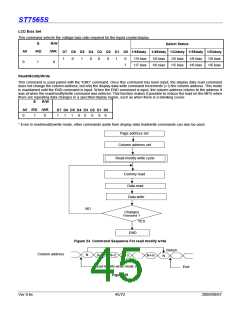
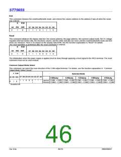
ST7565S
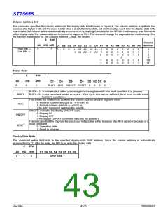
Column Address Set
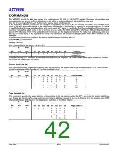
This command specifies the column address of the display data RAM shown in Figure 4. The column address is split into two
sections (the higher 4 bits and the lower 4 bits) when it is set (fundamentally, set continuously). Each time the display data RAM
is accessed, the column address automatically increments (+1), making it possible for the MPU to continuously read from/write
to the display data. The column address increment is topped at 83H. This does not change the page address continuously. See
the function explanation in “The Column Address Circuit,” for details.
E
R/W
Column
address
A0 /RD /WR
D7 D6 D5 D4 D3 D2 D1 D0 A7 A6 A5 A4 A3 A2 A1 A0
0
1
0
High bits →
Low bits →
0
0
0
1
A7 A6 A5 A4
0
0
0
0
0
0
0
0
0
0
0
0
0
0
0
0
0
0
0
0
1
0
1
0
0
1
2
0 A3 A2 A1 A0
↓
↓
1
1
0
0
0
0
0
0
0
0
0
0
1
1
0
1
130
131
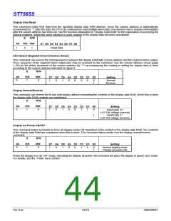
Status Read
E
R/W
A0
/RD
/WR
D7
D6
D5
D4
D3 D2 D1 D0
0
0
1
BUSY ADC ON/OFF RESET
0
0
0
0
BUSY = 1: it indicates that either processing is occurring internally or a reset condition is in process.
BUSY
BUSY = 0: A new command can be accepted . if the cycle time can be satisfied, there is no need to check
for BUSY conditions.
This shows the relationship between the column address and the segment driver.
0: Reverse (column address 131-n ↔ SEG n)
1: Normal (column address n ↔ SEG n)
(The ADC command switches the polarity.)
ON/OFF: indicates the display ON/OFF state.
0: Display ON
ADC
ON/OFF
RESET
1: Display OFF
(This display ON/OFF command switches the polarity.)
This indicates that the chip is in the process of initialization either because of a /RES signal or because of a
reset command.
0: Operating state
1: Reset in progress
Display Data Write
This command writes 8-bit data to the specified display data RAM address. Since the column address is automatically
incremented by “1” after the write, the MPU can write the display data.
E
R/W
A0 /RD /WR
D7 D6 D5 D4 D3 D2 D1 D0
1
1
0
Write data
Ver 0.6c
43/72
2009/09/07

 SITRONIX [ SITRONIX TECHNOLOGY CO., LTD. ]