ST7565S
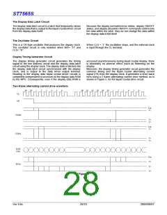
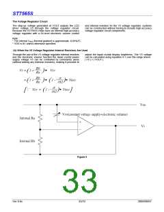
The LCD Driver Circuits
The LCD driver circuits generate four voltage levels to drive
the LCD. The combination of display data, the COM scan
signal and the FR signal produces the drive voltage of LCD.
Figure 6 shows examples of the SEG and COM output wave
form.
VDD
VSS
FR
COM0
V0
V1
V2
V3
V4
VSS
COM1
COM2
COM0
COM3
COM4
COM5
V0
V1
V2
V3
V4
VSS
COM1
COM6
COM7
COM8
V0
V1
V2
V3
V4
VSS
COM2
COM9
COM10
COM11
V0
V1
V2
V3
V4
VSS
COM12
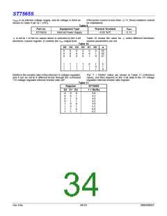
SEG0
COM13
COM14
V0
V1
V2
V3
V4
VSS
COM15
SEG1
SEGꢁ0
1
2
3
4
V0
V1
V2
V3
V4
COM0
to
SEG0
VSS
ꢂV4
ꢂV3
ꢂV2
ꢂV1
ꢂV0
V0
V1
V2
V3
V4
COM0
to
SEG1
VSS
ꢂV4
ꢂV3
ꢂV2
ꢂV1
ꢂV0
Figure 6
Ver 0.6c
30/72
2009/09/07

 SITRONIX [ SITRONIX TECHNOLOGY CO., LTD. ]