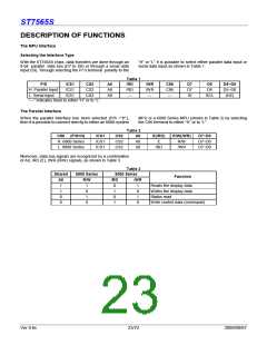
ST7565S
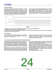
Display Data RAM
The display data RAM stores the dot data for the LCD. It has
a 65 (8 page x 8 bit +1) x 132 bit structure.
Moreover, reading from and writing to the display RAM from
the MPU side is performed through the I/O buffer, which is an
independent operation from signal reading for the liquid
crystal driver. Consequently, even if the display data RAM is
accessed asynchronously during liquid crystal display, it will
not cause adverse effects on the display (such as flickering).
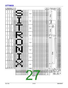
As is shown in Figure 3, the D7 to D0 display data from the
MPU corresponds to the LCD display common direction;
there are few constraints at the time of display data transfer
when multiple ST7565S are used, thus and display structures
can be created easily and with a high degree of freedom.
D0
D1
D2
D3
D4
-
0
1
0
0
1
1
0
0
1
0
1
0
0
1
0
1
0
0
1
0
0
0
0
0
0
COM0
COM1
COM2
COM3
COM4
-
Display data RAM
Liquid crystal display
Figure 3
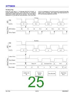
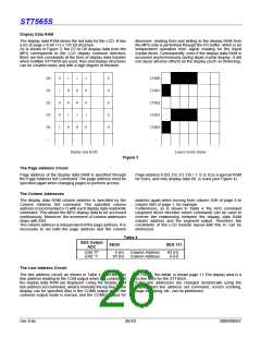
The Page Address Circuit
Page address of the display data RAM is specified through
the Page Address Set Command. The page address must be
specified again when changing pages to perform access.
Page address 8 (D3, D2, D1, D0 = 1, 0, 0, 0) is a special RAM
for icons, and only display data D0 is used (see Figure 4).
The Column Addresses
The display data RAM column address is specified by the
Column Address Set command. The specified column
address is incremented (+1) with each display data read/write
command. This allows the MPU display data to be accessed
continuously. Moreover, the increment of column addresses
stops with 83H.
address again when moving from column 83H of page 0 to
column 00H of page 1, for example.
Furthermore, as is shown in Table 4, the ADC command
(segment driver direction select command) can be used to
reverse the relationship between the display data RAM
column address and the segment output. Therefore, the
constraints of the LCD module layout with this IC can be
minimized.
The column address is independent of the page address. It is
necessary to set both the page address and the column
Table 4
SEG Output
ADC
SEG0
SEG 131
(D0) “0”
(D0) “1”
0 (H)
83 (H)
Column Address
Column Address
83 (H)
0 (H)
The Line Address Circuit
The line address circuit, as shown in Table 4, specifies the
line address relating to the COM output when the contents of
the display data RAM are displayed. Using the display start
line address set command, what is normally the top line of the
display can be specified (this is the COM0 output when the
common output mode is normal, and the COM63 output for
ST7565S , the detail is shown page.11 The display area is a
65 line area for the ST7565S.
If the line addresses are changed dynamically using the
display start line address set command, screen scrolling,
page swapping, etc. can be performed.
Ver 0.6c
26/72
2009/09/07

 SITRONIX [ SITRONIX TECHNOLOGY CO., LTD. ]