ST7565S
The Display Data Latch Circuit
The display data latch circuit is a latch that temporarily stores
the display data that is output to the liquid crystal driver circuit
from the display data RAM.
Because the display normal/reverse status, display ON/OFF
status, and display all points ON/OFF commands control only
the data within the latch, they do not change the data within
the display data RAM itself.
The Oscillator Circuit
This is a CR-type oscillator that produces the display clock.
The oscillator circuit is only enabled when M/S= “H” and
CLS= “H”.
When CLS = “L” the oscillation stops, and the external clock
is input through the CL terminal.
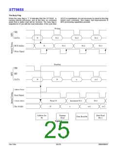
Display Timing Generator Circuit
The display timing generator circuit generates the timing
signal to the line address circuit and the display data latch
circuit using the display clock. The display data is latched into
the display data latch circuit synchronized with the display
clock, and is output to the data driver output terminal.
Reading to the display data liquid crystal driver circuits is
completely independent of accesses to the display data RAM
by the MPU. Consequently, even if the display data RAM is
accessed asynchronously during liquid crystal display, there
is absolutely no adverse effect (such as flickering) on the
display.
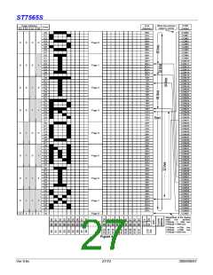
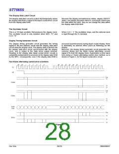
Moreover, the display timing generator circuit generates the
common timing and the liquid crystal alternating current
signal (FR) from the display clock. It generates a drive wave
form using a 2 frame alternating current drive method, as is
shown in Figure 5, for the liquid crystal drive circuit.
Two-frame alternating current drive waveform
64 65
1
2
3
4
5
6
60 61 62 63 64 65
1
2
3
4
5
6
CL
FR
V
DD
V
1
COM0
V
V
4
5
V
DD
V
1
COM1
V
V
4
5
RAM
Data
V
DD
V
2
3
5
SEGn
V
V
Figure 5
Ver 0.6c
28/72
2009/09/07

 SITRONIX [ SITRONIX TECHNOLOGY CO., LTD. ]