ST7565S
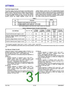
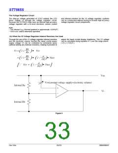
The Power Supply Circuits
The power supply circuits are low-power consumption power
supply circuits that generate the voltage levels required for
the LCD drivers. They are Booster circuits, voltage regulator
circuits, and voltage follower circuits. They are only enabled
in master operation. The power supply circuits can turn the
Booster circuits, the voltage regulator circuits, and the
voltage follower circuits ON or OFF independently through
the use of the Power Control Set command. Consequently, it
is possible to make an external power supply and the internal
power supply function somewhat in parallel. Table 7 shows
the Power Control Set Command 3-bit data control function,
and Table 8 shows reference combinations.
Table 7
Status
bit
Function
“1”
“0”
D2
D1
D0
Booster circuit control bit (V/B circuit)
Voltage regulator circuit control bit (V/R circuit)
Voltage follower circuit control bit (V/F circuit)
ON
ON
ON
OFF
OFF
OFF
The Control Details of Each Bit of the Power Control Set Command
Table 8: Reference Power Circuits Combinations
External
power
input
Voltage
Booster
Voltage
Regulator Follower
Voltage
Booster
Capacitor
Use Settings
D2 D1 D0
Only the internal power supply is used
1
0
0
0
1
1
0
0
1
1
1
0
ON
ON
ON
ON
ON
VSS2
Used
Open
Open
Open
Only the voltage regulator and follower
circuits are used
VOUT,
VSS2
OFF
OFF
OFF
Only the voltage follower circuit is used
Only the external power supply is used
OFF
OFF
ON
V5, VSS2
V1 to V5
OFF
* The “Booster Capacitor” refers CAP1+, CAP1–, CAP2+, CAP2–, and CAP3–.
* The other combinations (not shown above) are also possible, but they are not recommended because they have no practical
use.
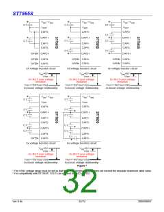
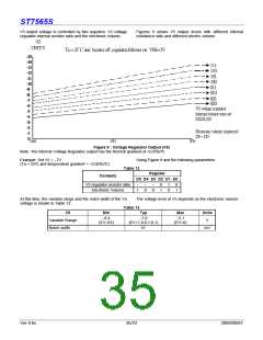
The Step-up Voltage Circuits
Using the booster circuits equipped within ST7565S, it is
possible to generate a boosted voltage which is 2X, 3X, 4X,
5X or 6X step-up of the VDD – VSS2 voltage levels.
The circuit connection is described below and illustrated in
Figure 7.
4X step-up:
Connect capacitor C1 between CAP1+ and CAP1–,
between CAP2+ and CAP2–, between CAP1+ and
CAP3–, and between VSS2 and VOUT.
It produces a voltage level in the negative direction at the
VOUT terminal, and which is 4 times the voltage level
between VDD and VSS2.
6X step-up:
Connect capacitor C1 between CAP1+ and CAP1–,
between CAP2+ and CAP2–, between CAP1+ and
CAP3–, between CAP2+ and CAP4–, between CAP1+
and CAP5–, and between VSS2 and VOUT.
It produces a voltage level in the negative direction at the
VOUT terminal, and which is 6 times the voltage level
between VDD and VSS2.
3X step-up:
Connect capacitor C1 between CAP1+ and CAP1–,
between CAP2+ and CAP2–, between VSS2 and VOUT,
and short CAP3– with VOUT.
It produces voltages level in the negative direction at the
VOUT terminal, and which is 3 times the voltage level
between VDD and VSS2.
5X step-up:
Connect capacitor C1 between CAP1+ and CAP1–,
between CAP2+ and CAP2–, between CAP1+ and
CAP3–, between CAP2+ and CAP4–, and between
VSS2 and VOUT.
2X step-up:
Connect capacitor C1 between CAP1+ and CAP1–, and
between VSS2 and VOUT, and short CAP2– with CAP3–
and VOUT (leave CAP2+ open).
It produces a voltage level in the negative direction at the
VOUT terminal, and which is 5 times the voltage level
between VDD and VSS2.
It produces a voltage in the negative direction at the
VOUT terminal, and which is twice the voltage level
between VDD and VSS2.
Ver 0.6c
31/72
2009/09/07

 SITRONIX [ SITRONIX TECHNOLOGY CO., LTD. ]