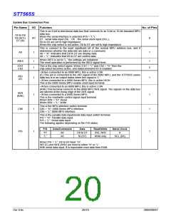
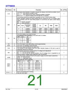
ST7565S
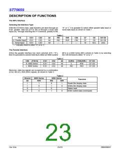
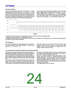
The Serial Interface
When the serial interface has been selected (P/S = “L”) then
when the chip is in active state (/CS1 = “L” and CS2 = “H”) the
serial data input (SI) and the serial clock input (SCL) can be
received. The serial data is read from the serial data input pin
in the rising edge of the serial clocks D7, D6 through D0, in
this order. This data is converted to 8 bits parallel data in the
rising edge of the eighth serial clock for the processing.
The A0 input is used to determine whether or the serial data
input is display data or command data; when A0 = “H”, the
data is display data, and when A0 = “L” then the data is
command data. The A0 input is read and used for detection
every 8th rising edge of the serial clock after the chip
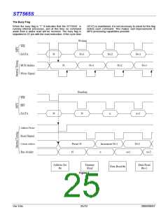
becomes active. Figure 1 is a serial interface signal chart.
CS1
CS2
SI
SCL
A0
D7
D6
D5
D4
D3
D2
D1
D0
D7
D6
D5
D4
D3
D2
1
2
3
4
5
6
7
8
9
10
11
12
13
14
Figure 1
* When the chip is not active, the shift registers and the counter are reset to their initial states.
* Reading is not possible while in serial interface mode.
* Caution is required on the SCL signal when it comes to line-end reflections and external noise. We recommend that operation
be rechecked on the actual equipment.
The Chip Select
The ST7565S have two chip select terminals: /CS1 and CS2.
The MPU interface or the serial interface is enabled only
when /CS1 = “L” and CS2 = “H”.
When the chip select is inactive, D0 to D7 enter a high
impedance state, and the A0, /RD, and /WR inputs are
inactive. When the serial interface is selected, the shift
register and the counter are reset.
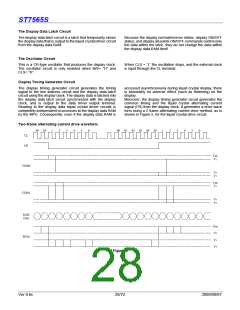
The Accessing the Display Data RAM and the Internal Registers
Data transfer at a higher speed is ensured since the MPU is
required to satisfy the cycle time (tCYC) requirement alone in
accessing the ST7565S. Wait time may not be considered.
And, in the ST7565S, each time data is sent from the MPU, a
type of pipeline process between LSIs is performed through
the bus holder attached to the internal data bus. Internal data
bus.
For example, when the MPU writes data to the display data
RAM, once the data is stored in the bus holder, then it is
written to the display data RAM before the next data write
cycle. Moreover, when the MPU reads the display data RAM,
the first data read cycle (dummy) stores the read data in the
bus holder, and then the data is read from the bus holder to
the system bus at the next data read cycle.
There is a certain restriction in the read sequence of the
display data RAM. Please be advised that data of the
specified address is not generated by the read instruction
issued immediately after the address setup. This data is
generated in data read of the second time. Thus, a dummy
read is required whenever the address setup or write cycle
operation is conducted.
This relationship is shown in Figure 2.
Ver 0.6c
24/72
2009/09/07

 SITRONIX [ SITRONIX TECHNOLOGY CO., LTD. ]