ST7565S
LCD Driver Pins
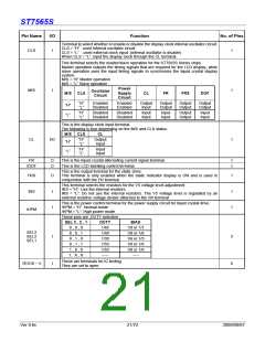
Pin Name
I/O
Function
No. of Pins
These are the LCD segment drive outputs. Through a combination of the contents of the
display RAM and with the FR signal, a single level is selected from VDD, V2, V3, and V5.
Output Voltage
RAM DATA
FR
Normal Display Reverse Display
SEG0
to
SEG131
H
H
L
H
L
VDD
V5
V2
V3
O
132
H
L
V2
VDD
V5
L
V3
Power save
VDD
Through a combination of the contents of the scan data and with the FR signal, a single
level is selected from VDD, V1, V4, and V5.
Scan Data
FR
H
L
Output Voltage
COM0
to
COMn
H
H
L
V5
VDD
V1
O
O
67
H
L
L
V4
Power save
VDD
These are the COM output terminals for the indicator. Both terminals output the same
signal.
COMS
2
Leave these open if they are not used.
I/O PIN ITO Resister Limitation
PIN Name
ITO Resister
FR, /DOF, C86, P/S, M/S, /HPM,SEL1…SEL3, CLS, IRS
TEST0…6
VDD, VSS, VSS2, VOUT, VR, VRS
No Limitation
Floating
<100Ω
V1, V2, V3, V4, V5, CAP1+, CAP1
–
, CAP2+, CAP2
–
, CAP3
–
, CAP4–, CAP5
–
<300Ω
/CS1, CS2, CL, E, R/W, A0, D0…D7,
/RES
<1KΩ
<10KΩ
Ver 0.6c
22/72
2009/09/07

 SITRONIX [ SITRONIX TECHNOLOGY CO., LTD. ]