ST7565S
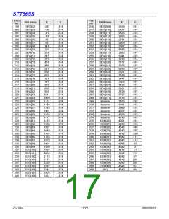
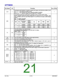
Pin Name
I/O
Function
No. of Pins
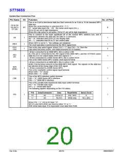
Terminal to select whether or enable or disable the display clock internal oscillator circuit.
CLS = “H” : used Internal oscillator circuit .
CLS = “L” : used external clock input .(internal oscillator is disable)
When CLS = “L”, input the display clock through the CL terminal.
CLS
I
1
This terminal selects the master/slave operation for the ST7565S Series chips.
Master operation outputs the timing signals that are required for the LCD display, while
slave operation uses the input timing signals to synchronize the liquid crystal display
system.
M/S = “H” Master operation
M/S = “L” Slave operation
Power
Supply
Circuit
M/S
I
1
Oscillator
Circuit
M/S CLS
CL
FR
FRS
DOF
“H”
Enabled
Disabled
Enabled
Enabled
Output
Input
Output
Output
Output
Output
Output
Output
“H”
“L”
“H”
Disabled
Disabled
Disabled
Disabled
Input
Input
Input
Input
Output
Output
Input
Input
“L”
“L”
This is the display clock input terminal.
The following is true depending on the M/S and CLS status.
M/S CLS
CL
CL
I/O
1
“H”
Output
Input
“H”
“L”
“H”
Input
Input
“L”
“L”
FR
O
O
This is the liquid crystal alternating current signal terminal.
This is the LCD blanking control terminal.
1
1
/DOF
This is the output terminal for the static drive.
FRS
IRS
O
This terminal is only enabled when the static indicator display is ON and is used in
conjunction with the FR terminal.
1
1
1
This terminal selects the resistors for the V5 voltage level adjustment.
IRS = “H”: Use the internal resistors
IRS = “L”: Do not use the internal resistors. The V5 voltage level is regulated by an
external resistive voltage divider attached to the VR terminal
I
This is the power control terminal for the power supply circuit for liquid crystal drive.
/HPM = “H”: Normal mode
/HPM = “L”: High power mode
I
/HPM
These pins are DUTY selection.
SEL 3 , 2 , 1
0 , 0 , 0
DUTY
1/65
1/49
1/33
1/55
1/53
-----
BIAS
1/9 or 1/7
1/8 or 1/6
1/6 or 1/5
1/8 or 1/6
1/8 or 1/6
-----
SEL3
SEL2
SEL1
0 , 0 , 1
I
I
3
6
0 , 1 , 0
0 , 1 , 1
1 , 0 , 0
1, X , X
These are terminals for IC testing.
They are set to open.
TEST0 ~ 5
Ver 0.6c
21/72
2009/09/07

 SITRONIX [ SITRONIX TECHNOLOGY CO., LTD. ]