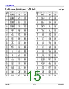
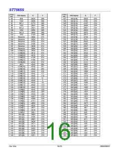
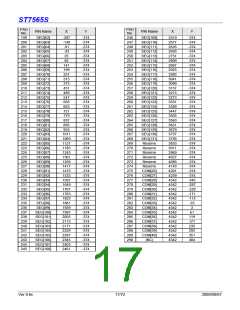
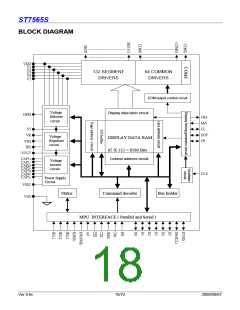
ST7565S
PIN DESCRIPTIONS
Power Supply Pins
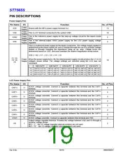
Pin Name
I/O
Function
No. of Pins
Power
Supply
VDD
Shared with the MPU power supply terminal Vcc.
13
Power
Supply
VSS
VSS2
VRS
This is a 0V terminal connected to the system GND.
10
2
Power This is the reference power supply for the step-up voltage circuit for the liquid crystal
Supply drive.
Power This is the internal-output VREG power supply for the LCD power supply voltage
Supply regulator.
2
This is a multi-level power supply for the liquid crystal drive. The voltage Supply applied is
determined by the liquid crystal cell, and is changed through the use of a resistive voltage
divided or through changing the impedance using an op. amp. Voltage levels are
determined based on VDD, and must maintain the relative magnitudes shown below.
VDD (= V0) ≧V1 ≧V2 ≧V3 ≧V4 ≧V5
V1, V2,
V3, V4,
V5
Power When the power supply turns ON, the internal power supply circuits produce the V1 to V4
Supply voltages shown below. The voltage settings are selected using the LCD bias set
command.
10
1/65 DUTY
1/49 DUTY
1/33 DUTY
1/55 DUTY
1/53 DUTY
V1 1/9*V5,1/7*V5 1/8*V5,1/6*V5 1/6*V5,1/5*V5 1/8*V5,1/6*V5 1/8*V5,1/6*V5
V2 2/9*V5,2/7*V5 2/8*V5,2/6*V5 2/6*V5,2/5*V5 2/8*V5,2/6*V5 2/8*V5,2/6*V5
V3 7/9*V5,5/7*V5 6/8*V5,4/6*V5 4/6*V5,3/5*V5 6/8*V5,4/6*V5 6/8*V5,4/6*V5
V4 8/9*V5,6/7*V5 7/8*V5,5/6*V5 5/6*V5,4/5*V5 7/8*V5,5/6*V5 7/8*V5,5/6*V5
LCD Power Supply Pins
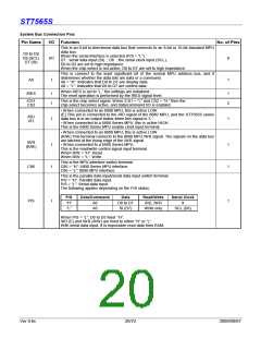
Pin Name
I/O
Function
No. of Pins
DC/DC voltage converter. Connect a capacitor between this terminal and the CAP1-
terminal.
CAP1+
O
4
DC/DC voltage converter. Connect a capacitor between this terminal and the CAP1+
terminal.
CAP1–
CAP2+
CAP2–
CAP3–
CAP4–
O
O
O
O
O
2
2
2
2
2
DC/DC voltage converter. Connect a capacitor between this terminal and the CAP2-
terminal.
DC/DC voltage converter. Connect a capacitor between this terminal and the CAP2+
terminal.
DC/DC voltage converter. Connect a capacitor between this terminal and the CAP1+
terminal.
DC/DC voltage converter. Connect a capacitor between this terminal and the CAP2+
terminal.
DC/DC voltage converter. Connect a capacitor between this terminal and the CAP1+
terminal.
CAP5–
VOUT
O
O
2
2
DC/DC voltage converter. Connect a capacitor between this terminal and VSS.
Output voltage regulator terminal. Provides the voltage between VDD and V5 through a
resistive voltage divider.
IRS = “L” : the V5 voltage regulator internal resistors are not used .
IRS = “H” : the V5 voltage regulator internal resistors are used .
VR
I
2
Ver 0.6c
19/72
2009/09/07

 SITRONIX [ SITRONIX TECHNOLOGY CO., LTD. ]