SiI 1161 PanelLink Receiver
Data Sheet
Feature Information
HSYNC De-jitter Function
HSYNC de-jitter enables the SiI 1161 to operate properly even when the HSYNC signal contains jitter. Pin 1 is
used to enable or disable this circuit. Tying this pin high enables the HSYNC de-jitter circuitry while tying it low
disables the circuitry. The HSYNC de-jitter circuitry operates normally with most VESA standard timings. In most
modes, HSYNC and VSYNC total times and front and back porch times are multiples of four pixel times. If the
timings are not a multiple of four, operation is not guaranteed and the HSYNC de-jitter circuitry should be turned
off. When HSYNC de-jitter is enabled, the circuitry will introduce anywhere from 1 to 4 CLK delays in the HSYNC
signal relative to the output data.
Clock Detect Function
The SiI 1161 includes a power saving feature: power down with clock detect circuit. The SiI 1161 will go into a low
power mode when there is no video clock coming from the transmitter. In this mode, the entire chip is powered
down except the clock detect circuitry. During this mode, digital I/O are set to a high impedance (tri-state) mode.
The SCDT pin is driven LOW. A weak internal pull-down device brings each output to ground. The device power
down and wake-up times are shown in Figure 11 and Figure 12.
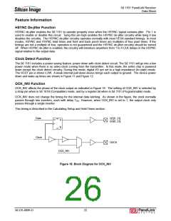
OCK_INV Function
OCK_INV affects the phase of the clock output as indicated in Figure 18. The setting of OCK_INV is selected by
a strap pin when in SiI 161B (Compatible) mode, and by a register bit when in SiI 1161 (Programmable) mode.
OCK_INV does not change the timing for the internal data latching. As shown in the figure, the clock normally
passes through two inverters, each with delay TINV. However, when OCK_INV is set to 1, the output clock only
passes through a single inverter.
This timing is described in the Calculating Setup and Hold Times section.
Data
SET
QE[0..23]
QO[0..23]
D
Q
Q
CLR
Clock
ODCK
OCK_INV
Figure 18. Block Diagram for OCK_INV
SiI-DS-0096-D
22

 SILICONIMAGE [ Silicon image ]