SiI 1161 PanelLink Receiver
Data Sheet
Pin Descriptions
Output Pins
Pin Name
QE23-
QE0
Pin #
See
Type
Description
Out
Output Even Data[23:0] corresponds to 24-bit pixel data for one pixel per clock input mode
and to the first 24-bit pixel data for two pixels per clock mode.
SiI 1161
Output data is synchronized with output data clock (ODCK).
Pin
Refer to the TFT Panel Data Mapping section, which tabulates the relationship between the
input data to the transmitter and output data from the receiver.
Diagram
A low level on PD# or PDO# will put the output drivers into a high impedance (tri-state) mode.
A weak internal pull-down device brings each output to ground.
QO23-
QO0
See
Out
Output Odd Data[23:0] corresponds to the second 24-bit pixel data for two pixels per clock
mode. During one pixel per clock mode, these outputs are driven low.
SiI 1161
Output data is synchronized with output data clock (ODCK).
Pin
Refer to the TFT Panel Data Mapping section, which tabulates the relationship between the
input data to the transmitter and output data from the receiver.
Diagram
A low level on PD# or PDO# will put the output drivers into a high impedance (tri-state) mode.
A weak internal pull-down device brings each output to ground.
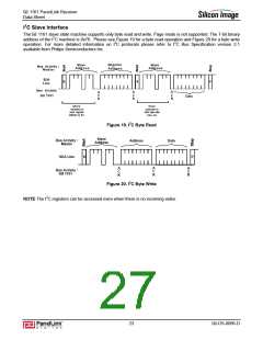
ODCK
DE
44
46
Out
Out
Output Data Clock. This output can be inverted using the OCK_INV pin. A low level on PD# or
PDO# will put the output driver into a high impedance (tri-state) mode. A weak internal pull-
down device brings the output to ground.
Output Data Enable. This signal qualifies the active data area. A HIGH level signifies active
display time and a LOW level signifies blanking time. This output signal is synchronized with
the output data. A low level on PD# or PDO# will put the output driver into a high impedance
(tri-state) mode. A weak internal pull-down device brings the output to ground.
HSYNC
VSYNC
CTL1
48
47
40
41
42
Out
Horizontal Sync output control signal.
Vertical Sync output control signal.
General output control signal 1. This output is not powered down by PDO#.
General output control signal 2.
CTL2
CTL3
General output control signal 3.
A low level on PD# or PDO# will put the output drivers (except CTL1 by PDO#) into a high
impedance (tri-state) mode. A weak internal pull-down device brings each output to ground.
Differential Signal Data Pins
Pin Name
RX0+
RX0-
Pin #
90
Type
Description
Analog Receiver Differential Data Pins. TMDS Low Voltage Differential Signal input data pairs.
91
RX1+
RX1-
85
86
RX2+
RX2-
80
81
RXC+
RXC-
93
94
Analog Receiver Differential Clock Pins. TMDS Low Voltage Differential Signal input clock pair.
EXT_RES
96
Analog
Impedance Matching Control. An external 390Ω resistor must be connected between AVCC
and this pin.
19
SiI-DS-0096-D

 SILICONIMAGE [ Silicon image ]