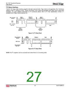
SiI 1161 PanelLink Receiver
Data Sheet
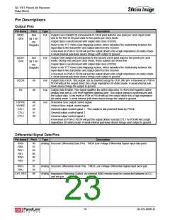
Configuration Pins
Pin Name
Pin # Type
Description
MODE
99
In
Mode Select Pin. Used to select between drop-in strap-selected operation, or register-
programmable operation. To activate register-programmable operation, tie both pin 99 and
pin 7 LOW. Refer to Selecting SiI 1161 (Programmable) Mode on page 31 for more details.
HIGH=161B (Compatible) Mode – strap selections are used to set part operation. Internal
registers controlling non strap-selectable functions are reset to their default values.
LOW=1161 (Programmable) Mode – I2C registers are used to program part operation.
OCK_INV
SCL
100
In
ODCK Polarity. A LOW level selects normal ODCK output. A HIGH level selects inverted
ODCK output. All other output signals are unaffected by this pin. They will maintain the same
timing no matter the setting of OCK_INV pin
I2C Port Clock. When pins 99 and 7 are tied LOW, pin 100 functions as an I2C port input
clock. The slave I2C function does not ever try to extend cycles by pulling this pin low, so the
pin remains input-only at all times. Refer to Selecting SiI 1161 (Programmable) Mode on
page 31 for more details. This pin accepts 3.3V signaling only; it is not 5V-tolerant.
PIXS
4
7
In
In
Pixel Select. A LOW level indicates one pixel (up to 24-bits) per clock mode using QE[23:0].
A HIGH level indicates two pixels (up to 48-bits) per clock mode using QE[23:0] for first pixel
and QO[23:0] for second pixel.
STAG_OUT#
Staggered Output. A HIGH level selects normal simultaneous outputs on all odd and even
data lines. A LOW level selects staggered output drive. This function is only available in two
pixels per clock mode.
This pin must be tied LOW to put the receiver into I2C mode. Refer to Selecting SiI 1161
(Programmable) Mode on page 31 for more details.
I2C_MODE#
ST
3
1
In/
Output Drive. A HIGH level selects HIGH output drive strength. A LOW level selects LOW
Out output drive strength.
SDA
I2C Port Data. When pins 99 and 7 are tied LOW, pin 3 functions as an I2C port data I/O
signal. Refer to Selecting SiI 1161 (Programmable) Mode on page 31 for more details. This
pin accepts 3.3V signaling only; it is not 5V-tolerant. The I2C address of the SiI 1161 is 0x76
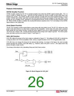
HS_DJTR
In
HSYNC De-jitter. This pin enables/disables the HSYNC de-jitter function. To enable the
HSYNC de-jitter function this pin should be HIGH. To disable the HSYNC de-jitter function this
pin should be LOW.
Power Management Pins
Pin Name Pin # Type
Description
SCDT
8
Out Sync Detect. A HIGH level is outputted when DE is actively toggling indicating that the link is
alive. A LOW level is outputted when DE is inactive, indicating the link is down. Can be
connected to PDO# to power down the outputs when DE is not detected. The SCDT output itself,
however, remains in the active mode at all times.
PDO#
9
In
Output Driver Power Down (active LOW). A HIGH level indicates normal operation. A LOW level
puts all the output drivers only (except SCDT and CTL1) into a high impedance (tri-state) mode.
A weak internal pull-down device brings each output to ground. PDO# is a sub-set of the PD#
description. The chip is not in power-down mode with this pin. SCDT and CTL1 are not tri-stated
by this pin. I2C access to the registers is available when PDO#=0.
PD#
2
In
Power Down (active LOW). A HIGH level indicates normal operation. A LOW level indicates
power down mode. During power down mode, all the output drivers are put into a high
impedance (tri-state) mode. A weak internal pull-down device brings each output to ground.
Additionally, all analog logic is powered down, and all inputs are disabled. Driving PD# LOW
disables all internal logic and outputs, including SCDT and clock detect functions; it also resets all
internal programmable registers to their default states. I2C access to the registers is disabled
when PD#=0.
SiI-DS-0096-D
20

 SILICONIMAGE [ Silicon image ]