SiI 1161 PanelLink Receiver
Data Sheet
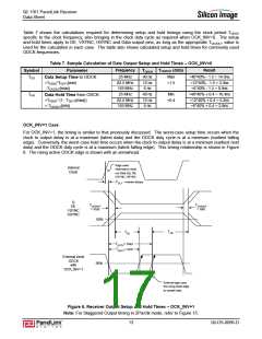
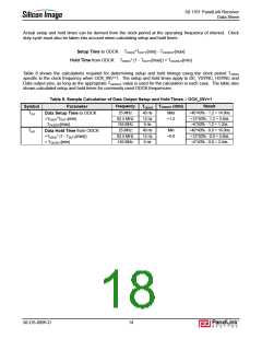
Table 7 shows the calculations required for determining setup and hold timings using the clock period TODCK
specific to the clock frequency, also bringing in the clock duty cycle as required when OCK_INV=0. The setup
and hold times apply to DE, VSYNC, HSYNC and Data output pins, as long as the appropriate TCK2OUT value is
used for the calculation in each case. The table also shows calculated setup and hold times for commonly used
ODCK frequencies.
Table 7. Sample Calculation of Data Output Setup and Hold Times – OCK_INV=0
Frequency
TCK2OUT (data)
Max
Result
Symbol
Parameter
TODCK
25 MHz
40 ns
=40*40% - 1.5 = 14.5ns
TSU
Data Setup Time to ODCK
=TODCK*TDUTY{min)
82.5 MHz
165 MHz
25 MHz
12 ns
6 ns
=1.5
=12*40% - 1.5 = 3.3ns
=6*40% - 1.5 = 0.9ns
=40*40% + 0.4 = 16.4ns
-TCK2OUT{max}
40 ns
Min
THD
Data Hold Time from ODCK
=TODCK* (1 - TDUTY{max})
+ TCK2OUT{min}
82.5 MHz
165 MHz
12 ns
6 ns
=0.4
=12*40% + 0.4 = 5.2ns
=6*40% + 0.4 = 2.8ns
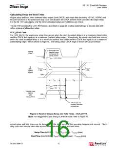
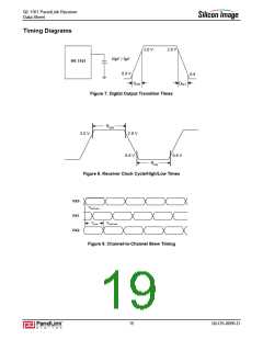
OCK_INV=1 Case
For OCK_INV=1, the timing is similar to that previously discussed. The worst-case setup time occurs when the
clock to output delay is at a maximum (latest data) and the ODCK duty cycle is at a minimum (earliest falling
edge). Conversely, the worst case hold time occurs when the clock to output delay is at a minimum (earliest next
data) and the ODCK duty cycle is at a maximum (latest falling edge). This timing relationship is shown in Figure
6. The rising active ODCK edge is shown with an arrowhead.
Edge used
Internal
internally to clock
Clock
out Data (Q), DE,
VSYNC, HSYNC
TDLY - inverter delays
Q
DE
VSYNC
HSYNC
TCK2OUT
= max
TCK2OUT
= min
50%
THD
TSU
T
DUTY= max
TDUTY= min
External clock
ODCK
50%
with
OCK_INV=1
External logic uses
this rising clock edge
to sample data
Figure 6. Receiver Output Setup and Hold Times – OCK_INV=1
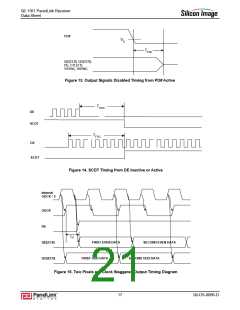
Note: For Staggered Output timing in 2Pix/clk mode, refer to Figure 15.
13
SiI-DS-0096-D

 SILICONIMAGE [ Silicon image ]