SiI 1161 PanelLink Receiver
Data Sheet
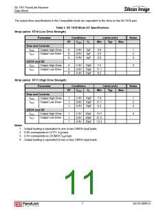
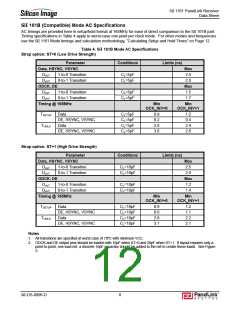
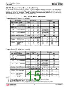
SiI 1161 (Programmable) Mode AC Specifications
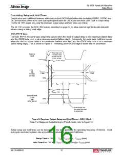
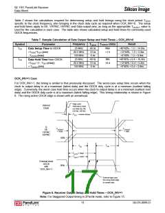
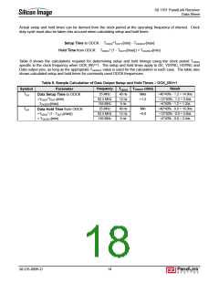
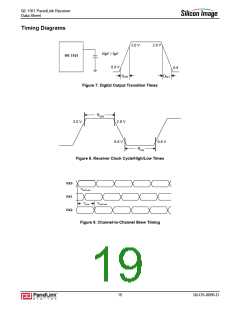
SiI 1161 Mode AC timings are based on “Clock to Output” (CK2OUT) timing measurements. This methodology
provides a precise means of calculating setup and hold at any frequency and in any chip operating mode. CL
indicates the load on the ODCK line. The load on the data/control line involved depends on CKST: for CKST=1,
the control/data pin load is CL; for CKST=0, the load is 2x CL.
Table 6. SiI 1161 Mode AC Specifications
Program Option: ST=0 (Low Drive Strength)
Parameter
Conditions
Limits (ns)
Data, HSYNC, VSYNC
CKST
ST
0
CL
5pF
5pF
CL
Max
2.5
DHLT
DLHT
1-to-0 Transition
X
0-to-1 Transition
X
0
2.0
ODCK, DE
DHLT
CKST
ST
0
Max
2.5
1-to-0 Transition
0-to-1 Transition
1
5pF
10pF
5pF
10pF
CL
1X clock drive
0
0
2X clock drive
1X clock drive
2X clock drive
Min
1.5
DLHT
1
0
0
2.7
0
1.7
Clock-to-Output Timing
CKST
ST
Max
OCK_INV Settingꢀ
0
1
0
1
TCK2OUT ODCK to Data
1
0
1
0
0
0
0
0
5pF
10pF
5pF
0.4
0.4
1.2
0.8
0.0
-0.1
0.2
0.1
1.5
1.5
2.2
2.2
1.2
1.0
2.0
1.7
TCK2OUT ODCK to DE,
HSYNC,
10pF
VSYNC
Program Option: ST=1 (High Drive Strength)
Parameter
Conditions
Limits (ns)
Data, HSYNC, VSYNC
CKST
ST
1
CL
Max
2.5
DHLT
DLHT
1-to-0 Transition
X
10pF
10pF
CL
0-to-1 Transition
X
1
2.0
ODCK, DE
DHLT
CKST
ST
1
Max
1.9
1-to-0 Transition
0-to-1 Transition
1
10pF
20pF
10pF
20pF
CL
2X clock drive
4X clock drive
2X clock drive
4X clock drive
Min
0
1
1.2
DLHT
1
0
1
1.7
1
1.4
Clock-to-Output Timing
CKST
ST
Max
OCK_INV Settingꢀ
0
1
0
1
TCK2OUT ODCK to Data
1
0
1
0
1
1
1
1
10pF
20pF
10pF
20pF
0.4
0.0
0.7
0.1
-0.2
-0.8
-0.3
-0.3
1.5
1.4
1.8
1.9
1.2
1.0
1.3
1.0
TCK2OUT ODCK to DE,
HSYNC,
VSYNC
Notes
1. Output loading is equivalent to one (5pF), two (10pF) or four (20pF) CMOS input loads.
2. All transition time specifications at 70°C, minimum VCC.
3. Timing specifications in Table 6 apply to both one pixel per clock and two pixel per clock modes.
11
SiI-DS-0096-D

 SILICONIMAGE [ Silicon image ]