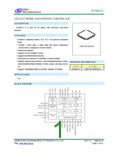
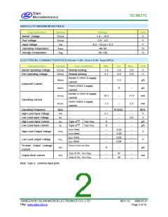
SC9821C
(Continued)
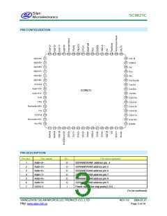
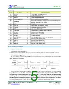
Pin No.
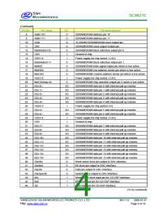
8
Pin name
Addr<10>
I/O
O
Pin descriptions
SDRAM/DRAM address pin 10
9
Addr<11>
SClk
O
SDRAM/DRAM address pin 11
10
O
16.9344M SDRAM/DRAM clock output pin.
SDRAM/DRAM clock output enable pin.
SDRAM/DRAM block selection output pin 0.
Ground of chip.
11
CKE
O
12
BankSelect<0>
VSS
O
13
I
14
VDD1.8
BankSelect<1>
NotWE
NotRAS
NotCAS
VDD1.8
NotCSArray<0>
DQ<0>
DQ<1>
DQ<2>
DQ<3>
DQ<4>
VDD3.3
DQ<5>
DQ<6>
VDD1.8
VSS
I
Power supply for chip kernel. (1.8V)
SDRAM/DRAM block selection output pin 1
15
O
16
O
SDRAM/DRAM write signal output pin which is low active.
SDRAM/DRAM row address strobe pin which is low active.
SDRAM/DRAM Column address strobe pin which is low active.
Power supply for chip kernel. (1.8V)
17
O
18
O
19
I
20
O
SDRAM/DRAM chip selection output pin 0 which is low active.
SDRAM/DRAM data pin 0 with internal pull up resistor.
SDRAM/DRAM data pin 1 with internal pull up resistor.
SDRAM/DRAM data pin 2 with internal pull up resistor.
SDRAM/DRAM data pin 3 with internal pull up resistor.
SDRAM/DRAM data pin 4 with internal pull up resistor.
Power supply for chip ports(3.3V).
21
I/O
I/O
I/O
I/O
I/O
I
22
23
24
25
26
27
I/O
I/O
I
SDRAM/DRAM data pin 5 with internal pull up resistor.
SDRAM/DRAM data pin 6 with internal pull up resistor.
Power supply for chip kernel. (1.8V).
28
29
30
I
Ground of chip.
31
DQ<7>
DQ<8>
DQ<9>
DQ<10>
DQ<11>
DQ<12>
DQ<13>
DQ<14>
DQ<15>
DacWs
DacBck
DacSd
I/O
I/O
I/O
I/O
I/O
I/O
I/O
I/O
I/O
O
SDRAM/DRAM data pin 7 with internal pull up resistor.
SDRAM/DRAM data pin 8 with internal pull up resistor.
SDRAM/DRAM data pin 9 with internal pull up resistor.
SDRAM/DRAM data pin 10 with internal pull up resistor.
SDRAM/DRAM data pin 11 with internal pull up resistor.
SDRAM/DRAM data pin 12 with internal pull up resistor.
SDRAM/DRAM data pin 13 with internal pull up resistor.
SDRAM/DRAM data pin 14 with internal pull up resistor.
SDRAM/DRAM data pin 15 with internal pull up resistor.
Word select clock pin output to DAC interface.
Bit clock pin output to DAC interface.
32
33
34
35
36
37
38
39
40
41
O
42
O
Data pin output to DAC interface.
43
DacSysClk
Ws
O
System clock output to DAC interface.
44
I
Word select clock input pin for CD•DSP interface.
Bit clock input pin for CD•DSP interface.
45
Bck
I
46
Sd
I
Data input pin for CD•DSP interface.
(To be continued)
HANGZHOU SILAN MICROELECTRONICS CO.,LTD
Http:
REV:1.0
2006.07.21
www.silan.com.cn
Page 4 of 18

 SILAN [ SILAN MICROELECTRONICS JOINT-STOCK ]