EFM32G Data Sheet
Pin Definitions
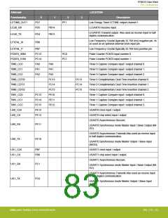
5.1.2 Alternate Functionality Pinout
A wide selection of alternate functionality is available for multiplexing to various pins. This is shown in the following table. The table
shows the name of the alternate functionality in the first column, followed by columns showing the possible LOCATION bitfield settings.
Note: Some functionality, such as analog interfaces, do not have alternate settings or a LOCATION bitfield. In these cases, the pinout
is shown in the column corresponding to LOCATION 0.
Table 5.2. Alternate functionality overview
Alternate
LOCATION
Functionality
ACMP0_CH0
ACMP0_CH1
ACMP0_O
0
1
2
3
Description
PC0
PC1
Analog comparator ACMP0, channel 0.
Analog comparator ACMP0, channel 1.
PE13
PC13
PC14
PC15
PF2
Analog comparator ACMP0, digital output.
Analog comparator ACMP1, channel 5.
ACMP1_CH5
ACMP1_CH6
ACMP1_CH7
ACMP1_O
Analog comparator ACMP1, channel 6.
Analog comparator ACMP1, channel 7.
Analog comparator ACMP1, digital output.
Analog to digital converter ADC0, input channel number 4.
Analog to digital converter ADC0, input channel number 5.
Analog to digital converter ADC0, input channel number 6.
Analog to digital converter ADC0, input channel number 7.
Bootloader RX.
ADC0_CH4
ADC0_CH5
ADC0_CH6
ADC0_CH7
BOOT_RX
PD4
PD5
PD6
PD7
PE11
PE10
PA2
BOOT_TX
Bootloader TX.
CMU_CLK0
CMU_CLK1
DAC0_OUT0
Clock Management Unit, clock output number 0.
Clock Management Unit, clock output number 1.
Digital to Analog Converter DAC0 output channel number 0.
Debug-interface Serial Wire clock input.
PA1
PB11
DBG_SWCLK
DBG_SWDIO
PF0
PF1
PF0
PF1
Note that this function is enabled to pin out of reset, and has a
built-in pull down.
Debug-interface Serial Wire data input / output.
Note that this function is enabled to pin out of reset, and has a
built-in pull up.
Debug-interface Serial Wire viewer Output.
DBG_SWO
HFXTAL_N
PF2
PC15
Note that this function is not enabled after reset, and must be
enabled by software to be used.
High Frequency Crystal negative pin. Also used as external
optional clock input pin.
PB14
HFXTAL_P
I2C0_SCL
PB13
PA1
PA0
PD6
High Frequency Crystal positive pin.
I2C0 Serial Clock Line input / output.
I2C0 Serial Data input / output.
PD7
PD6
PB11
I2C0_SDA
LETIM0_OUT0
PF0
Low Energy Timer LETIM0, output channel 0.
silabs.com | Building a more connected world.
Rev. 2.10 | 82

 SILICON [ SILICON ]