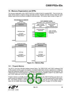
C8051F52x-53x
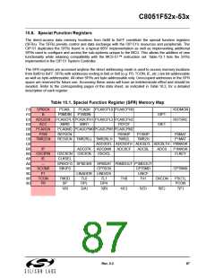
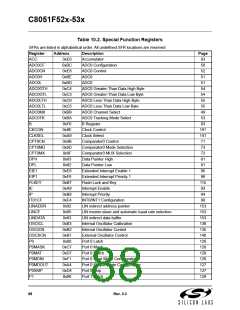
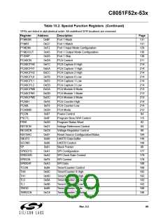
Table 10.2. Special Function Registers
SFRs are listed in alphabetical order. All undefined SFR locations are reserved
Register
ACC
Address
0xE0
0xBC
0xE8
0xBE
0xBD
0xC4
0xC3
0xC6
0xC5
0xBB
0xBA
0xF0
0x8E
0xA9
0x9B
0x9D
0x9F
0x83
0x82
0xE6
0xF6
0xB7
0xA8
0xB8
0xE4
0x92
0x95
0x93
0xB3
0xB2
0xB1
0x80
0xC7
0xD7
0xF1
0xA4
0xD4
0x90
Description
Page
83
Accumulator
ADC0CF
ADC0CN
ADC0H
ADC0L
ADC0GTH
ADC0GTL
ADC0LTH
ADC0LTL
ADC0MX
ADC0TK
B
ADC0 Configuration
ADC0 Control
50
52
ADC0
51
ADC0
51
ADC0 Greater-Than Data High Byte
ADC0 Greater-Than Data Low Byte
ADC0 Less-Than Data High Byte
ADC0 Less-Than Data Low Byte
ADC0 Channel Select
ADC0 Tracking Mode Select
B Register
54
54
55
55
49
53
83
CKCON
CLKSEL
CPT0CN
CPT0MD
CPT0MX
DPH
Clock Control
191
141
71
Clock Select
Comparator0 Control
Comparator0 Mode Selection
Comparator0 MUX Selection
Data Pointer High
73
72
81
DPL
Data Pointer Low
81
EIE1
Extended Interrupt Enable 1
Extended Interrupt Priority 1
Flash Lock and Key
95
EIP1
96
FLKEY
IE
115
93
Interrupt Enable
IP
Interrupt Priority
94
IT01CF
LINADDR
LINCF
INT0/INT1 Configuration
LIN indirect address pointer
LIN master-slave and automatic baud rate selection
LIN indirect data buffer
Internal Oscillator Calibration
Internal Oscillator Control
External Oscillator Control
Port 0 Latch
98
153
153
153
136
135
140
126
128
128
126
127
127
129
LINDATA
OSCICL
OSCICN
OSCXCN
P0
P0MASK
P0MAT
P0MDIN
P0MDOUT
P0SKIP
P1
Port 0 Mask
Port 0 Match
Port 0 Input Mode Configuration
Port 0 Output Mode Configuration
Port 0 Skip
Port 1 Latch
88
Rev. 0.3

 SILICON [ SILICON ]