C8051F52x-53x
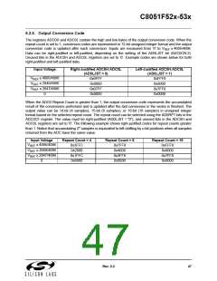
5.3.5. Output Conversion Code
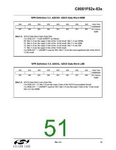
The registers ADC0H and ADC0L contain the high and low bytes of the output conversion code. When the
repeat count is set to 1, conversion codes are represented in 12-bit unsigned integer format and the output
conversion code is updated after each conversion. Inputs are measured from ‘0’ to V
x 4095/4096.
REF
Data can be right-justified or left-justified, depending on the setting of the AD0LJST bit (ADC0CN.2).
Unused bits in the ADC0H and ADC0L registers are set to ‘0’. Example codes are shown below for both
right-justified and left-justified data.
Input Voltage
Right-Justified ADC0H:ADC0L
(AD0LJST = 0)
Left-Justified ADC0H:ADC0L
(AD0LJST = 1)
V
V
V
x 4095/4096
0x0FFF
0x0800
0x07FF
0x0000
0xFFF0
0x8000
0x7FF0
0x0000
REF
x 2048/4096
REF
x 2047/4096
REF
0
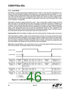
When the ADC0 Repeat Count is greater than 1, the output conversion code represents the accumulated
result of the conversions performed and is updated after the last conversion in the series is finished. The
output value can be 14-bit (4 samples), 15-bit (8 samples), or 16-bit (16 samples) in unsigned integer
format based on the selected repeat count. The repeat count can be selected using the AD0RPT bits in the
ADC0CF register. The value must be right-justified (AD0LJST = “0”), and unused bits in the ADC0H and
ADC0L registers are set to '0'. The following example shows right-justified codes for repeat counts greater
n
than 1. Notice that accumulating 2 samples is equivalent to left-shifting by n bit positions when all samples
returned from the ADC have the same value.
Input Voltage
Repeat Count = 4
0x3FFC
Repeat Count = 8
0x7FF8
Repeat Count = 16
0xFFF0
V
V
V
x 4095/4096
REF
x 2048/4096
0x2000
0x4000
0x8000
REF
x 2047/4096
0x1FFC
0x3FF8
0x7FF0
REF
0
0x0000
0x0000
0x0000
Rev. 0.3
47

 SILICON [ SILICON ]