C8051F52x-53x
5.3.1. Starting a Conversion
A conversion can be initiated in one of four ways, depending on the programmed states of the ADC0 Start
of Conversion Mode bits (AD0CM1–0) in register ADC0CN. Conversions may be initiated by one of the fol-
lowing:
•Writing a ‘1’ to the AD0BUSY bit of register ADC0CN
•A rising edge on the CNVSTR input signal (pin P0.6)
•A Timer 1 overflow (i.e., timed continuous conversions)
•A Timer 2 overflow (i.e., timed continuous conversions)
Writing a ‘1’ to AD0BUSY provides software control of ADC0 whereby conversions are performed "on-
demand.” During conversion, the AD0BUSY bit is set to logic 1 and reset to logic 0 when the conversion is
complete. The falling edge of AD0BUSY triggers an interrupt (when enabled) and sets the ADC0 interrupt
flag (AD0INT). Note: When polling for ADC conversion completions, the ADC0 interrupt flag (AD0INT)
should be used. Converted data is available in the ADC0 data registers, ADC0H:ADC0L, when bit AD0INT
is logic 1. Note that when Timer 2 overflows are used as the conversion source, Low Byte overflows are
used if Timer2 is in 8-bit mode; High byte overflows are used if Timer 2 is in 16-bit mode. See Section
“19. Timers” on page 185 for timer configuration.
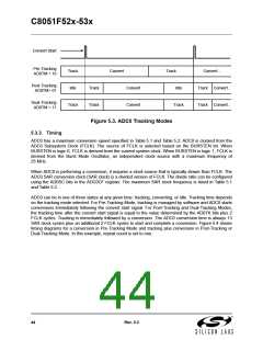
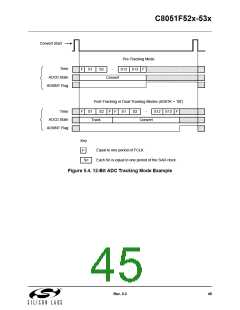
5.3.2. Tracking Modes
According to Table 5.1 and Table 5.2, each ADC0 conversion must be preceded by a minimum tracking
time for the converted result to be accurate. ADC0 has three tracking modes: Pre-Tracking, Post-Tracking,
and Dual-Tracking. Pre-Tracking Mode provides the minimum delay between the convert start signal and
end of conversion by tracking continuously before the convert start signal. This mode requires software
management in order to meet minimum tracking requirements. In Post-Tracking Mode, a programmable
tracking time starts after the convert start signal and is managed by hardware. Dual-Tracking Mode maxi-
mizes tracking time by tracking before and after the convert start signal. Figure 5.3 shows examples of the
three tracking modes.
Pre-Tracking Mode is selected when AD0TM is set to 10b. Conversions are started immediately following
the convert start signal. ADC0 is tracking continuously when not performing a conversion. Software must
allow at least the minimum tracking time between each end of conversion and the next convert start signal.
The minimum tracking time must also be met prior to the first convert start signal after ADC0 is enabled.
Post-Tracking Mode is selected when AD0TM is set to 01b. A programmable tracking time based on
AD0TK is started immediately following the convert start signal. Conversions are started after the pro-
grammed tracking time ends. After a conversion is complete, ADC0 does not track the input. Rather, the
sampling capacitor remains disconnected from the input making the input pin high-impedance until the
next convert start signal.
Dual-Tracking Mode is selected when AD0TM is set to 11b. A programmable tracking time based on
AD0TK is started immediately following the convert start signal. Conversions are started after the pro-
grammed tracking time ends. After a conversion is complete, ADC0 tracks continuously until the next con-
version is started.
Depending on the output connected to the ADC input, additional tracking time, more than is specified in
Table 5.1 and Table 5.2, may be required after changing MUX settings. See the settling time requirements
described in Section “5.3.6. Settling Time Requirements” on page 48.
Rev. 0.3
43

 SILICON [ SILICON ]