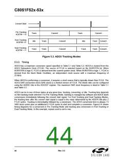
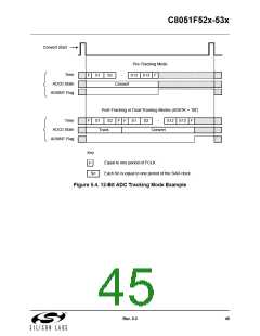
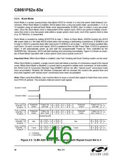
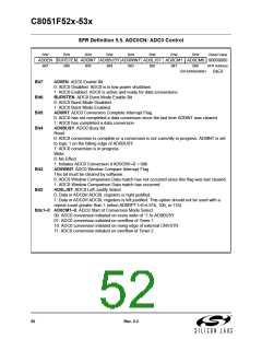
C8051F52x-53x
5.3.6. Settling Time Requirements
A minimum tracking time is required before an accurate conversion can be performed. This tracking time is
determined by the AMUX0 resistance, the ADC0 sampling capacitance, any external source resistance,
and the accuracy required for the conversion.
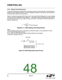
Figure 5.6 shows the equivalent ADC0 input circuit. The required ADC0 settling time for a given settling
accuracy (SA) may be approximated by Equation 5.1. When measuring the Temperature Sensor output or
V
with respect to GND, R
reduces to R
. See Table 5.1 and Table 5.2 for ADC0 minimum set-
DD
TOTAL
MUX
tling time requirements.
2n
SA
⎛
⎝
⎞
⎠
------
t = ln
× RTOTALCSAMPLE
Equation 5.1. ADC0 Settling Time Requirements
Where:
SA is the settling accuracy, given as a fraction of an LSB (for example, 0.25 to settle within 1/4 LSB)
t is the required settling time in seconds
R
is the sum of the AMUX0 resistance and any external source resistance.
TOTAL
n is the ADC resolution in bits (12).
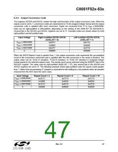
MUX Select
Px.x
RMUX = TBD
CSAMPLE = TBD
RCInput= RMUX * CSAMPLE
Figure 5.6. ADC0 Equivalent Input Circuits
48
Rev. 0.3

 SILICON [ SILICON ]