C8051F52x-53x
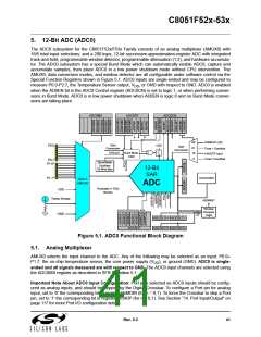
5. 12-Bit ADC (ADC0)
The ADC0 subsystem for the C8051F52x/F53x Family consists of an analog multiplexer (AMUX0) with
16/6 total input selections, and a 200 ksps, 12-bit successive-approximation-register ADC with integrated
track-and-hold, programmable window detector, programmable attenuation (1:2), and hardware accumula-
tor. The ADC0 subsystem has a special Burst Mode which can automatically enable ADC0, capture and
accumulate samples, then place ADC0 in a low power shutdown mode without CPU intervention. The
AMUX0, data conversion modes, and window detector are all configurable under software control via the
Special Function Registers shown in Figure 5.1. ADC0 inputs are single-ended and may be configured to
measure P0.0-P2.7, the Temperature Sensor output, V , or GND with respect to GND. ADC0 is enabled
DD
when the AD0EN bit in the ADC0 Control register (ADC0CN) is set to logic 1, or when performing conver-
sions in Burst Mode. ADC0 is in low power shutdown when AD0EN is logic 0 and no Burst Mode conver-
sions are taking place.
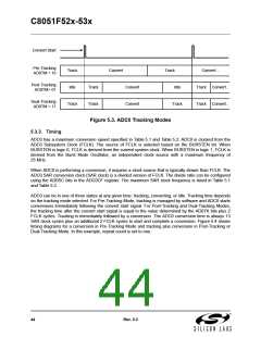
ADC0CN
ADC0MX
ADC0TK
00
01
10
11
AD0BUSY (W)
Start
Conversion
VDD
P0.0
Start
Conversion
Timer 1 Overflow
SYSCLK
Burst Mode
Logic
CNVSTR Input
Timer 2 Overflow
P0.7
P1.0*
Burst Mode
Oscillator
12-Bit
25 MHz Max
SAR
Accumulator
P1.7*
19-to-1
AMUX0
ADC
*Available in ‘F53x
devices
VDD
Temp Sensor
AD0WINT
Window
Compare
Logic
GND
32
ADC0LTH ADC0LTL
ADC0GTH ADC0GTL
ADC0CF
Figure 5.1. ADC0 Functional Block Diagram
5.1. Analog Multiplexer
AMUX0 selects the input channel to the ADC. Any of the following may be selected as an input: P0.0–
P1.7, the on-chip temperature sensor, the core power supply (V ), or ground (GND). ADC0 is single-
DD
ended and all signals measured are with respect to GND. The ADC0 input channels are selected using
the ADC0MX register as described in SFR Definition 5.1.
Important Note About ADC0 Input Configuration: Port pins selected as ADC0 inputs should be config-
ured as analog inputs, and should be skipped by the Digital Crossbar. To configure a Port pin for analog
input, set to ‘0’ the corresponding bit in register PnMDIN (for n = 0,1). To force the Crossbar to skip a Port
pin, set to ‘1’ the corresponding bit in register PnSKIP (for n = 0,1). See Section “14. Port Input/Output” on
page 117 for more Port I/O configuration details.
Rev. 0.3
41

 SILICON [ SILICON ]