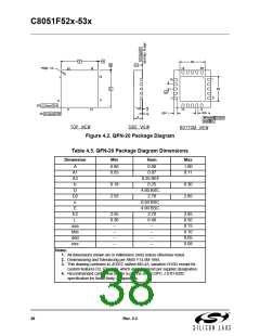
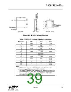
C8051F52x-53x
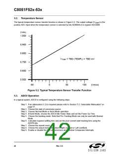
5.2. Temperature Sensor
The typical temperature sensor transfer function is shown in Figure 5.2. The output voltage (V
) is the
TEMP
positive ADC input when the temperature sensor is selected by bits AD0MX4–0 in register ADC0MX.
(Volts)
1.000
0.900
0.800
VTEMP = TBD (TEMPC) + TBD mV
0.700
0.600
0.500
(Celsius)
-50
Figure 5.2. Typical Temperature Sensor Transfer Function
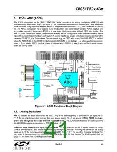
5.3. ADC0 Operation
0
50
100
In a typical system, ADC0 is configured using the following steps:
Step 1. If an attenuation (1:2) is required please refer to Section “5.5. Selectable Attenuation” on
page 57.
Step 2. Choose the start of conversion source.
Step 3. Choose Normal Mode or Burst Mode operation.
Step 4. If Burst Mode, choose the ADC0 Idle Power State and set the Power-Up Time.
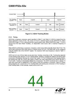
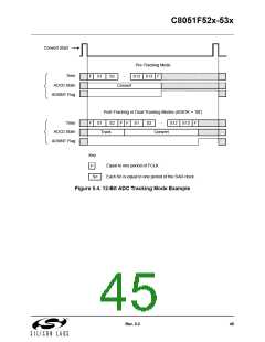
Step 5. Choose the tracking mode. Note that Pre-Tracking Mode can only be used with Normal
Mode.
Step 6. Calculate required settling time and set the post convert-start tracking time using the
AD0TK bits.
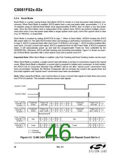
Step 7. Choose the repeat count.
Step 8. Choose the output word justification (Right-Justified or Left-Justified).
Step 9. Enable or disable the End of Conversion and Window Comparator Interrupts.
42
Rev. 0.3

 SILICON [ SILICON ]