C8051F52x-53x
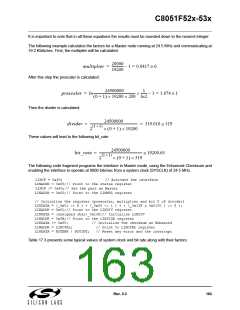
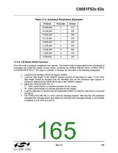
Table 17.4. Autobaud Parameters Examples
SYSCLK
25,000,000
24,500,000
24,000,000
22,118,400
16,000,000
12,250,000
12,000,000
11,059,200
8,000,000
Prescaler
Divider
312
1
1
1
1
1
0
0
0
0
306
300
276
200
306
300
276
200
17.4.5. LIN Master Mode Operation
Once the node is properly configured it can operate. The master node is responsible for the scheduling of
messages and sends the header of each frame, containing the SYNCH BREAK FIELD, SYNCH FIELD
and IDENTIFIER FIELD. The steps to schedule a message are described in the following paragraphs.
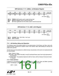
1. Load the 6-bit Identifier into the ID register (LINID).
2. Load the "data length" in the LINSIZE register (number of data bytes or value "1111b" if the
data length should be decoded from the identifier) and set the checksum type (classic or
enhanced, defined by the ENHCHK bit also in the LINSIZE register).
3. Adjust the TXRX bit (LINCTRL.5):
"1" - If the current frame is a transmit operation for the master.
"0" - If the current frame is a receive operation for the master.
4. Load the data bytes to transmit into the data buffer (LINDT1 to LINDT8, only if this is a transmit
operation).
5. The STREQ bit (LINCTRL) is set to start the message transfer. After that the LIN peripheral
schedules the message frame and request an interrupt if the message transfer is successfully
completed or if an error is occurred.
Rev. 0.3
165

 SILICON [ SILICON ]