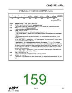
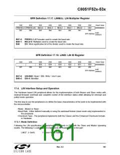
C8051F52x-53x
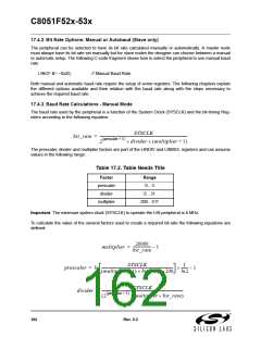
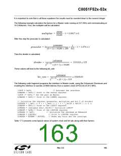
It is important to note that in all these equations the results must be rounded down to the nearest integer.
The following example calculates the factors for a Master node running at 24.5 MHz and communicating at
19.2 Kbits/sec. First, the multiplier will be calculated:
20000
19200
--------------
multiplier =
– 1 = 0.0417 ≅ 0
After this step the prescaler is calculated:
24500000
(0 + 1) × 19200 × 200 ln2
1
----------------------------------------------------- -------
prescaler = ln
×
– 1 = 1.674 ≅ 1
Then the divider is calculated:
24500000
(1 + 1) × (0 + 1) × 19200
------------------------------------------------------------
2
divider =
= 319.010 ≅ 319
These values will lead to the following bit_rate:
24500000
------------------------------------------------------
2
bit_rate =
≅ 19200.63
(1 + 1) × (0 + 1) × 319
The following code fragment programs the interface in Master mode, using the Enhanced Checksum and
enabling the interface to operate at 9600 bits/sec from a system clock (SYSCLK) of 24.5 MHz.
LINCF = 0x80;
// Activate the interface
LINADDR = 0x09;// Point to the status register
LINCF |= 0x40;// Set the part as Master
LINADDR = 0x0D;// Point to the LINMUL register
// Initialize the register (prescaler, multiplier and bit 8 of divider)
LINDATA = (_0x01 << 6 ) + (_0x00 << 1 ) + ( (_0x13F & 0x0100 ) >> 8 );
LINADDR = 0x0C;// Point to the LINDIV register
LINDATA = (unsigned char)_0x13F;// Initialize LINDIV
LINADDR = 0x0B;// Point to the LINSIZE register
LINDATA |= 0x80;
LINADDR = LINCTRL;
// Initialize the checksum as Enhanced
// Point to LINCTRL register
LINDATA = RSTERR | RSTINT;
// Reset any error and the interrupt
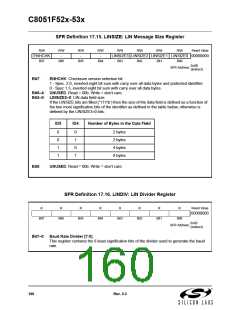
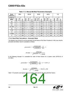
Table 17.3 presents some typical values of system clock and bit rate along with their factors:
Rev. 0.3
163

 SILICON [ SILICON ]