C8051F52x-53x
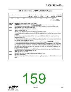
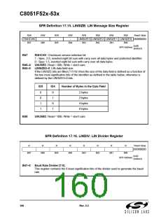
SFR Definition 17.15. LINSIZE: LIN Message Size Register
R/W
ENHCHK
Bit7
R/W
-
R/W
-
R/W
-
R/W
R/W
R/W
R/W
Reset Value
LINSIZE3 LINSIZE2 LINSIZE1 LINSIZE0 00000000
Bit6
Bit5
Bit4
Bit3
Bit2
Bit1
Bit0
0x0B
(indirect)
SFR Address:
Bit7:
ENHCHK: Checksum version selection bit
1 - Spec. 2.0, inverted eight bit sum with carry over all data bytes and protected identifier.
0 - Spec 1.3, inverted eight bit sum with carry over all data bytes.
Bit6–4: UNUSED. Read = 00b. Write = don’t care.
Bit3–0: LINSIZE3–0: LIN data field size.
If the LINSIZE bits are filled (“1111b’) then the size of the data field is defined as a function of
the two most significative bits of the identifier as defined in the table below, otherwise is
defined by the LINSIZE3–0 bits.
ID5
ID4
Number of Bytes in the Data Field
0
0
1
1
0
1
0
1
2 bytes
2 bytes
4 bytes
8 bytes
Bit0:
UNUSED. Read = 00b. Write = don’t care.
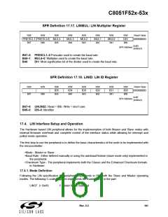
SFR Definition 17.16. LINDIV: LIN Divider Register
R
R
R
R
R
R
R
R
Reset Value
00000000
Bit7
Bit6
Bit5
Bit4
Bit3
Bit2
Bit1
Bit0
0x0C
(indirect)
SFR Address:
Bit7–0: Baud Rate Divider [7:0].
This register contains the 8 least significative bits of the divider used to generate the baud
rate.
160
Rev. 0.3

 SILICON [ SILICON ]