C8051F50x-F51x
Write to
0
PCA0CPLn
ENB
Reset
PCA0CPHn
PCA0CPLn
Write to
PCA0CPHn
ENB
COVF
1
PCA0PWM
A E C
R C O
S O V
E V F
L
PCA0CPMn
C C
L L
S S
E E
L L
1 0
P E C C M T P E
W C A A A O W C
M O P P T G M C
1 M P N n n n F
6 n n n
n
n
0
x
0
0
0
0 0 x 0
x
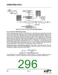
8-bit
Comparator
match
SET
CLR
CEXn
Enable
S
R
Q
Q
Crossbar
Port I/O
PCA Timebase
PCA0L
Overflow
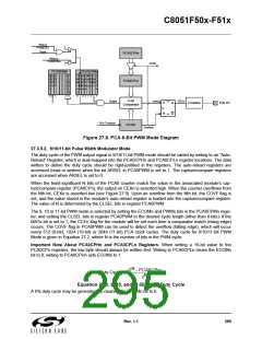
Figure 27.8. PCA 8-Bit PWM Mode Diagram
27.3.5.2. 9/10/11-bit Pulse Width Modulator Mode
The duty cycle of the PWM output signal in 9/10/11-bit PWM mode should be varied by writing to an “Auto-
Reload” Register, which is dual-mapped into the PCA0CPHn and PCA0CPLn register locations. The data
written to define the duty cycle should be right-justified in the registers. The auto-reload registers are
accessed (read or written) when the bit ARSEL in PCA0PWM is set to 1. The capture/compare registers
are accessed when ARSEL is set to 0.
When the least-significant N bits of the PCA0 counter match the value in the associated module’s cap-
ture/compare register (PCA0CPn), the output on CEXn is asserted high. When the counter overflows from
the Nth bit, CEXn is asserted low (see Figure 27.9). Upon an overflow from the Nth bit, the COVF flag is
set, and the value stored in the module’s auto-reload register is loaded into the capture/compare register.
The value of N is determined by the CLSEL bits in register PCA0PWM.
The 9, 10 or 11-bit PWM mode is selected by setting the ECOMn and PWMn bits in the PCA0CPMn regis-
ter, and setting the CLSEL bits in register PCA0PWM to the desired cycle length (other than 8-bits). If the
MATn bit is set to 1, the CCFn flag for the module will be set each time a comparator match (rising edge)
occurs. The COVF flag in PCA0PWM can be used to detect the overflow (falling edge), which will occur
every 512 (9-bit), 1024 (10-bit) or 2048 (11-bit) PCA clock cycles. The duty cycle for 9/10/11-Bit PWM
Mode is given in Equation 27.2, where N is the number of bits in the PWM cycle.
Important Note About PCA0CPHn and PCA0CPLn Registers: When writing a 16-bit value to the
PCA0CPn registers, the low byte should always be written first. Writing to PCA0CPLn clears the ECOMn
bit to 0; writing to PCA0CPHn sets ECOMn to 1.
N
2 – PCA0CPn
Duty Cycle = -----------------------------------------------
N
2
Equation 27.3. 9, 10, and 11-Bit PWM Duty Cycle
A 0% duty cycle may be generated by clearing the ECOMn bit to 0.
Rev. 1.1
295

 SILICON [ SILICON ]