LOW CURRENT CONSUMPTION HIGH RIPPLE-REJECTION LOW DROPOUT CMOS VOLTAGE REGULATOR
Rev.2.3_01
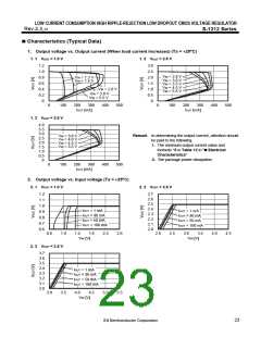
S-1312 Series
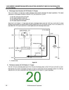
3. ON / OFF pin
This pin starts and stops the regulator.
When the ON / OFF pin is set to OFF level, the entire internal circuit stops operating, and the built-in
P-channel MOS FET output transistor between the VIN pin and the VOUT pin is turned off, reducing current
consumption significantly.
Note that the current consumption increases when a voltage of 0.25 V to VIN − 0.3 V is applied to the ON / OFF pin.
The ON / OFF pin is configured as shown in Figure 18 and Figure 19.
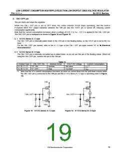
3. 1 S-1312 Series A / C type
The ON / OFF pin is internally pulled down to the VSS pin in the floating status, so the VOUT pin is set to the VSS
level.
For the ON / OFF pin current, refer to the A / C type of the ON / OFF pin input current "H" in " Electrical
Characteristics".
3. 2 S-1312 Series B / D type
The ON / OFF pin is internally not pulled up or pulled down, so do not use this pin in the floating status. When not
using the ON / OFF pin, connect the pin to the VIN pin.
Table 13
Product Type
A / B / C / D
A / B / C / D
ON / OFF Pin
"H": ON
"L": OFF
Internal Circuit
Operate
Stop
VOUT Pin Voltage
Set value
Current Consumption
*1
ISS1
ISS2
VSS level
*1. Note that the IC's current consumption increases as much as current flows into the pull-down resistor when
the ON / OFF pin is connected to the VIN pin and the S-1312 Series A / C type is operating (refer to Figure
18).
VIN
VIN
ON / OFF
ON / OFF
VSS
VSS
Figure 18 S-1312 Series A / C type
Figure 19 S-1312 Series B / D type
19

 SII [ SEIKO INSTRUMENTS INC ]