LOW CURRENT CONSUMPTION HIGH RIPPLE-REJECTION LOW DROPOUT CMOS VOLTAGE REGULATOR
Rev.2.3_01
S-1312 Series
Operation
1. Basic operation
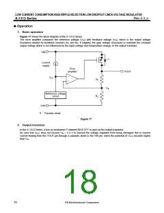
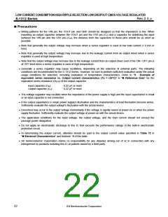
Figure 17 shows the block diagram of the S-1312 Series.
The error amplifier compares the reference voltage (Vref) with feedback voltage (Vfb), which is the output voltage
resistance-divided by feedback resistors (Rs and Rf). It supplies the gate voltage necessary to maintain the constant
output voltage which is not influenced by the input voltage and temperature change, to the output transistor.
VIN
*1
Current
supply
Error
amplifier
VOUT
−
+
Vref
Rf
Vfb
Reference voltage
circuit
Rs
VSS
*1. Parasitic diode
Figure 17
2. Output transistor
In the S-1312 Series, a low on-resistance P-channel MOS FET is used as the output transistor.
Be sure that VOUT does not exceed VIN + 0.3 V to prevent the voltage regulator from being damaged due to inverse
current flowing from the VOUT pin through a parasitic diode to the VIN pin, when the potential of VOUT became higher
than VIN.
18

 SII [ SEIKO INSTRUMENTS INC ]