140dB Range (1nA to 10mA)
SGM834A
Logarithmic Current-to-Voltage Converter
APPLICATION INFORMATION
Shielding, guarding, filtering and proper diode biasing
are critical factors to minimize the noise voltage
coupled to the INPT, especially when the diode current
is low and the feedback signal through Q1 is high. The
diode resistive leakage (dark current) along with the
multiplication and self-demodulation in the compensation
multipliers can increase the errors significantly.
Therefore, proper shielding, filtering and diode bias are
essential before feeding the current signal for
conversion.
negative feedback loop. Setting the corner frequency of
external R1-C1 network to smaller values will cause
slower settling at lower IPD currents but quicker settling
at high currents. So the span of the desired operating
range and the stability (or settling) of the converter
need to be compromised depending on the application
requirements.
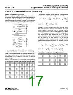
Figure 9 shows some additional circuits for the
photodiode bias and IPD signal filtering. The CPDB-RPDB
low pass R-C network reduces the bandwidth of the
adaptive biasing loop and helps the stability at high
currents. The CPD-RPD RC low pass filter network
averages the IPD before feeding it to the converter to
suppress the error caused by the multiplication
self-demodulation at low bit rate data communication
applications.
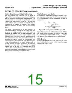
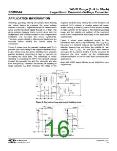
Figure 8 shows how the parasitic leakage and R1-C1
network can cause delay in the negative feedback loop.
It also shows how the active shielding loop provides
positive feedback (bootstrap) at high IPD currents by
increasing the diode bias. The advantage of active
shielding is insulating the INPT from ground leakage
through the parasitic CPG and RPG elements and also
from EMI pick-up. However, the penalty of shielding is
larger parasitic CPS that increases the delay in the
Note that VLOG output filtering is not helpful for error
suppression.
0.6V
-
VPDB
300Ω
QM
0.5V
10kΩ
EMI
INPT
CPS
RPS
-
+
C1
VSUM
CS
TCA
Q1
R1
GND
CPG
RPG
Figure 8. Conversion Loop and Active Shielding Loop
RPDB
VPDB
VPDB
CPDB
RPD
CPD
INPT
INPT
C1
C1
R1
VSUM
CS
VSUM
CS
R1
GND
GND
Figure 9. Filtering the VPDB and IPD
SG Micro Corp
www.sg-micro.com
FEBRUARY 2022
16

 SGMICRO [ Shengbang Microelectronics Co, Ltd ]