140dB Range (1nA to 10mA)
SGM834A
Logarithmic Current-to-Voltage Converter
DETAILED DESCRIPTION (continued)
Active Shielding and Adaptive Biasing
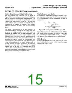
The INPT voltage level is kept at 0.5V as shown in
Figure 2. The same voltage is connected to VSUM pins
that are located on the two sides of the INPT pin. It is
recommended to surround the photodiode anode
copper stripe that connects to the INPT pin, with the
same voltage that is available on VSUM pins to
minimize the IPD leakage by creating a zero voltage
difference between the INPT and the surrounding
guard.
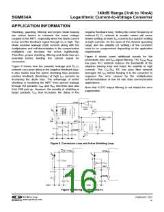
The Reference and Buffer
A 2V reference and a buffer operational amplifier (OPA)
are integrated on the chip. The OPA can be used for
VLOG conditioning or as a conventional op-amp or
comparator.
RINREF
ROUT
VINREF
A
VOUT
+
VIN
VOUTREF
ROUTREF
RIN
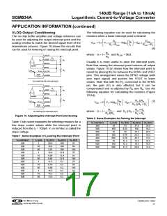
The QM is a current mirror to Q1 and its current is
proportional to the Q1 current. The QM current flows into
a current to voltage amplifier with a 0.6V offset to
generate an adaptive bias for the photodiode. The
photodiode bias increases from 100mV (= 0.6V - 0.5V)
minimum up to 300mV/mA × IPD (mA), or the headroom
limit, whichever is less. The reverse bias voltage is
increased at higher currents to compensate the
resistive drops in the photodiode. Note that for higher
range of the input current, the supply voltage needs to
be high enough for proper operation of the adaptive
bias. For example, with a 10mA input, the supply
voltage must be at least 3.7V, otherwise the VPDB
output will be saturated that may cause measurement
error. An external bias can be applied to VSUM if the
INPT voltage needs to be changed from 0.5V.
Figure 7. Re-scaling and Level-Shifting by an OPA
Figure 7 shows how the buffer can be used to shift the
VIN signal that is referenced to VINREF to a re-scaled
VOUT output signal referenced to the VOUTREF voltage.
The gain and level-shift are set by the four resistors.
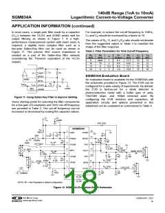
Chip Enable
Pulling up the PWDN pin to logic high level will power
down and disable the device. In this mode, the supply
current drops to 9μA (TYP).
SG Micro Corp
www.sg-micro.com
FEBRUARY 2022
15

 SGMICRO [ Shengbang Microelectronics Co, Ltd ]