140dB Range (1nA to 10mA)
SGM834A
Logarithmic Current-to-Voltage Converter
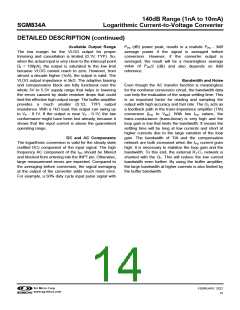
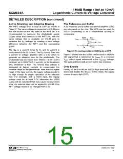
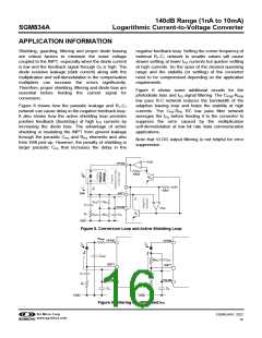
APPLICATION INFORMATION (continued)
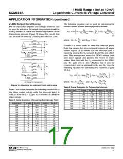
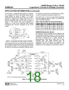
Table 4. Evaluation Board Configuration Options
Component
VS, AGND
SW1, R10
R1, R2
Function
Default Condition
Positive Supply and Ground Pins
Device Enable: With SW1 switch in the “0” position, the PWDN pin is grounded and the SW1 = Installed
SGM834A operates in normal mode. R10 = 10kΩ
Buffer Amplifier Gain/Slope Adjustment: The logarithmic slope of the SGM834A can be R1 = Open
NA
changed by gain-setting resistors (R1 and R2) of the buffer amplifier.
R2 = 0Ω
R3 = NP
Intercept Adjustment: These resistors can apply DC offset to the buffer amplifier inputs to
adjust the effective logarithmic intercept.
R3, R4
R4 = NP
R5 = R6 = NP
R7 = R8 = NP
C1 = 0.1nF
C2 = 1nF
R5, R6, R7, R8
Bias Adjustment: The VSUM and INPT voltages can be set by these resistors.
C1, C2, C3, C4, C9 Power Supply, VREF and PWDN Decoupling Capacitors.
C3 = 0.1μF
C4 = 4.7Μf
C9 = 10nF
Photodiode Bias Output Decoupling Capacitor: Provides high frequency decoupling for the
adaptive bias output at pin VPDB pin.
C10
C12
C10 = 0.1μF
C12 = 0.1μF
VSUM Decoupling Capacitor.
C5 = C6 = NP
C7 = C8 = NP
C5, C6, C7, C8, R11, Output Filter Configuration: These components can be used to implement a variety of filter
R11 = R13 = 0Ω
R12, R13, R14
configurations, from a simple low-pass RC filter to a three-pole Sallen-Key filter.
R12 = NP
R14 = 0Ω
Input Filtering: This RC network sets the essential HF compensation at the input pin R15 = 750Ω
(INPT). C11 = 470pF
Guard/Shield Options: The shells of the SMA input connectors for the photodiode and bias LK1 = Installed
can be either connected to active shield driver on the VSUM pin or connected to ground. LK2 = Open
R15, C11
LK1, LK2
REVISION HISTORY
NOTE: Page numbers for previous revisions may differ from page numbers in the current version.
Changes from Original (FEBRUARY 2022) to REV.A
Page
Changed from product preview to production data.............................................................................................................................................All
SG Micro Corp
www.sg-micro.com
FEBRUARY 2022
19

 SGMICRO [ Shengbang Microelectronics Co, Ltd ]