140dB Range (1nA to 10mA)
SGM834A
Logarithmic Current-to-Voltage Converter
APPLICATION INFORMATION (continued)
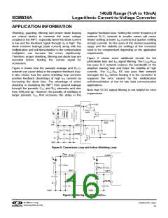
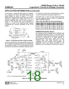
In most cases, a single-pole filter made by a capacitor
(CFLT) between the VLOG and AGND works well for
output filtering as shown in Figure 1. If a high-
performance measurement system with lower noise is
required, a slightly more complex filter such as a
two-pole Sallen-Key filter can be used as shown in
Figure 11. The precise 5kΩ source impedance is
needed as a part of the Sallen-Key filter network
(considering the Thevenin equivalent of the VLOG
output).
For example, to reduce the cut-off frequency to 100Hz,
CA and CB should be increased by a factor of 10.
The values of RD, G, and CA/CB ratio should not deviate
from the suggested values in Table 3 to maintain the
shape of the filter response.
Table 3. Filter Parameters for 1kHz Cut-off Frequency
RA
(kΩ)
RB
(kΩ)
VY
(V/dec)
RD
(kΩ)
CA
(nF)
CB
(nF)
G
0
open
10
8
1
2
0.2
0.4
0.5
1.0
11.3
6.02
12.1
10.0
12
33
33
33
12
22
18
18
10
12
24
2.5
5
VOUT
6
CB
RA
2V
VREF
BFNG
-
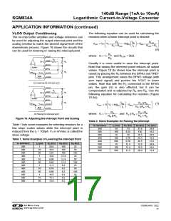
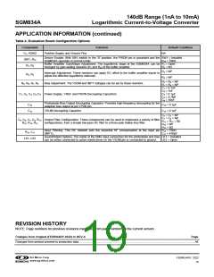
SGM834A Evaluation Board
CA
Buffer
An evaluation board is available for the SGM834A with
the schematic provided in Figure 12. The EVB can be
configured for a wide variety of experiments. By default,
the EVB is factory-set for a diode detector in
photoconductive mode with a buffer gain of unity,
10mV/dB slope, and 100pA intercept point. By
configuring the EVB resistors and capacitors, all
application circuits and options presented in this
datasheet can be evaluated as summarized in Table 4.
BFIN
RD
ILOG
VLOG
VLOG
AGND
RB
5kΩ
AGND
Figure 11. Using Sallen-Key Filter to Improve Settling
Some starting points for selecting the filter components
for a few gain (G) examples and 1kHz cut-off frequency
are provided in Table 3. The cut-off frequency can be
increased or decreased by scaling the capacitor values.
J1
J2
+VS
AGND
FB1 0.0Ω
SGM834A
R10
10kΩ
1
2
3
4
5
6
7
14
GND
AGND
R1
NP
C1
0.1nF
C2
1nF
SW1
13
12
11
10
9
PWDN
VSUM
INPT
BFNG
VPS
C13
NP
R2
0.0Ω
PDWN
R5
NP
R7
Open
R7 NP
LK2 Open
C3
C4
0.1μF
4.7μF
R13 0.0Ω
1 INPT
J4
VOUT
VPS
1
Buffer OUT
J6
R8 NP
R15
750Ω
C8
NP
C7
NP
R12
NP
VSUM
VPDB
VREF
R6
NP
C11
470pF
C12
0.1μF
R
11 0.0Ω
VPDB
J5
1
BFIN
VLOG
C10
0.1μF
R14 0.0Ω
C6
8
1
LOG OUT
J7
LK1
Installed
C9
10nF
C5
NP
NP
R4 NP
R3 NP
NOTE: NP = Not Populated in default configuration
Figure 12. SGM834A Evaluation Board Schematic
SG Micro Corp
www.sg-micro.com
FEBRUARY 2022
18

 SGMICRO [ Shengbang Microelectronics Co, Ltd ]