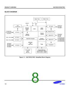
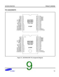
PRODUCT OVERVIEW
POWER-DOWN
S3C70F2/C70F4/P70F4
To reduce power consumption, there are two power-down modes: idle and stop. The IDLE instruction initiates idle
mode; the STOP instruction initiates stop mode.
In idle mode, the CPU clock stops while peripherals continue to operate normally. In stop mode, system clock
oscillation stops completely, halts all operations except for a few basic peripheral functions. A power-down is
terminated either by a RESET or by an interrupt (with exception of the external interrupt INT0).
RESET
When RESET is input during normal operation or during power-down mode, a reset operation is initiated and the
CPU enters idle mode. When the standard oscillation stabilization time interval (31.3 ms at 4.19 MHz) has
elapsed, normal CPU operation resumes.
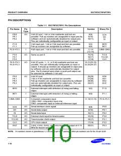
I/O PORTS
The S3C70F2/C70F4 has seven I/O ports. Pin addresses for all I/O ports are mapped to locations FF0H–FF6H
in bank 15 of the RAM. There are 6 input pins and 18 configurable I/O pins including 8 high current I/O pins for a
total of 24 I/O pins. The contents of I/O port pin latches can be read, written, or tested at the corresponding
address using bit manipulation instructions.
TIMERS and TIMER/COUNTER
The timer function has three main components: an 8-bit basic timer, an 8-bit timer/counter, and a watch timer.
The 8-bit basic timer generates interrupt requests at precise intervals, based on the selected internal clock
frequency.
The programmable 8-bit timer/counter is used for counting events, modifying internal clock frequencies, and
dividing external clock signals. The 8-bit timer/counter generates a clock signal (SCK) for the serial I/O interface.
The watch timer consists of an 8-bit watch timer mode register, a clock selector, and a frequency divider circuit.
Its functions include real-time, watch-time measurement, and clock generation for frequency output for buzzer
sound.
SERIAL I/O INTERFACE
The serial I/O interface supports the transmission or reception of 8-bit serial data with an external device. The
serial interface has the following functional components:
— 8-bit mode register
— Clock selector circuit
— 8-bit buffer register
— 3-bit serial clock counter
The serial I/O circuit can be set to transmit-and-receive, or to receive-only mode. MSB-first or LSB-first
transmission is also selectable.
The serial interface can operate with an internal or an external clock source, or using the clock signal generated
by the 8-bit timer/counter. Transmission frequency can be modified by setting the appropriate bits in the SIO
mode register.
1-6

 SAMSUNG [ SAMSUNG ]