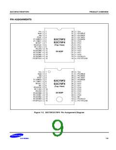
S3C70F2/C70F4/P70F4
PRODUCT OVERVIEW
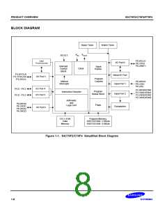
FUNCTION OVERVIEW
SAM47 CPU
All S3C7-series microcontrollers have the advanced SAM47 CPU core. The SAM47 CPU can directly address up
to 32 K bytes of program memory. The arithmetic logic unit (ALU) performs 4-bit addition, subtraction, logical,
and shift-and-rotate operations in one instruction cycle and most 8-bit arithmetic and logical operations in two
cycles.
CPU REGISTERS
Program Counter
A 11-bit program counter (PC) stores addresses for instruction fetch during program execution. Usually, the PC is
incremented by the number of bytes of the instruction being fetched. An exception is the 1-byte instruction REF
which is used to reference instructions stored in a look-up table in the ROM. Whenever a reset operation or an
interrupt occurs, bits PC11 through PC0 are set to the vector address. Bit PC13–12 is reserved to support future
expansion of the device's ROM size.
Stack Pointer
An 8-bit stack pointer (SP) stores addresses for stack operations. The stack area is located in the general-
purpose data memory bank 0. The SP is read or written by 8-bit instructions and SP bit 0 must always be set to
logic zero.
During an interrupt or a subroutine call, the PC value and the program status word (PSW) are saved to the stack
area in RAM. When the service routine has completed, the values referenced by the stack pointer are restored.
Then, the next instruction is executed.
The stack pointer can access the stack regardless of data memory access enable flag status. Since the reset
value of the stack pointer is not defined in firmware, it is recommended that the stack pointer be initialized to 00H
by program code. This sets the first register of the stack area to data memory location 0FFH.
PROGRAM MEMORY
In its standard configuration, the 4096 ´ 8-bit ROM is divided into three functional areas:
— 16-byte area for vector addresses
— 96-byte instruction reference area
— 1920-byte general purpose area (S3C70F2)
— 3968-byte general purpose area (S3C70F4)
The vector address area is used mostly during reset operations and interrupts. These 16 bytes can also be used
as general-purpose ROM.
The REF instruction references 2 ´ 1-byte and 2-byte instructions stored in locations 0020H–007FH. The REF
instruction can also reference 3-byte instructions such as JP or CALL. In order for REF to be able to reference
these instructions, however, JP or CALL must be shortened to a 2-byte format. To do this, JP or CALL is written
to the reference area with the format TJP or TCALL instead of the normal instruction name. Unused locations in
the instruction reference area can be allocated to general-purpose use.
1-3

 SAMSUNG [ SAMSUNG ]