PRODUCT OVERVIEW
S3C70F2/C70F4/P70F4
FEATURES SUMMARY
Memory
Bit Sequential Carrier
·
Supports 16-bit serial data transfer in arbitrary
format
·
·
512 ´ 4-bit data memory (RAM)
2048 ´ 8-bit program memory (ROM):S3C70F2
4096 ´ 8-bit program memory (ROM):S3C70F4
Interrupts
·
·
·
Two external interrupt vectors
24 I/O Pins
Three internal interrupt vectors
Two quasi-interrupts
·
I/O: 18 pins, including 8 high current pins
Input only: 6 pins
·
Memory-Mapped I/O Structure
Data memory bank 15
Comparator
·
·
4-channel mode:
Internal reference (4-bit resolution)
16-step variable reference voltage
Two Power-Down Modes
·
3-channel mode:
External reference
150 mV resolution (worst case)
·
·
Idle mode: Only CPU clock stops
Stop mode: System clock stops
8-bit Basic Timer
OSCILLATION SOURCES
·
·
Programmable interval timer
Watch-dog timer
·
·
·
Crystal, Ceramic for system clock
Crystal/ceramic: 0.4 - 6.0 MHz
CPU clock divider circuit (by 4. 8, or 64)
8-bit Timer/Counter 0
·
·
Programmable interval timer
Instruction Execution Times
External event counter function
Timer/counter clock output to TCLO0 pin
·
·
0.95, 1.91, 15.3 µs at 4.19 MHz
0.67, 1.33, 10.7 µs at 6.0 MHz
Watch Timer
·
Time interval generation: 0.5 s, 3.9 ms at 4.19
MHz
Operating Temperature
° °
– 40 C to 85 C
·
·
4 frequency outputs to BUZ pin
Operating Voltage Range
1.8 V to 5.5 V
8-bit Serial I/O Interface
·
·
·
·
·
8-bit transmit/receive mode
8-bit receive-only mode
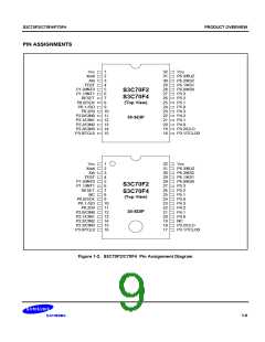
Package Type
30 SDIP, 32 SOP
LSB-first or MSB-first transmission selectable
Internal or external clock source
·
1-2

 SAMSUNG [ SAMSUNG ]