S3C70F2/C70F4/P70F4
PRODUCT OVERVIEW
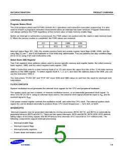
CONTROL REGISTERS
Program Status Word
The 8-bit program status word (PSW) controls ALU operations and instruction execution sequencing. It is also
used to restore a program's execution environment when an interrupt has been serviced. Program instructions
can always address the PSW regardless of the current value of data memory enable flags.
Before an interrupt or subroutine is processed, the PSW values are pushed onto the stack in data memory bank
0. When the service routine is completed, the PSW values are restored.
IS1
C
IS0
EMB
SC1
ERB
SC0
SC2
Interrupt status flags (IS1, IS0), the enable memory bank and enable register bank flags (EMB, ERB), and the
carry flag (C) are 1- and 4-bit read/write or 8-bit read-only addressable. You can address the skip condition flags
(SC0–SC2) using 8-bit read instructions only.
Select Bank (SB) Register
Two 4-bit registers store address values used to access specific memory and register banks: the select memory
bank register, SMB, and the select register bank register, SRB.
'SMB n' instruction selects a data memory bank (0 or 15) and stores the upper four bits of the 12-bit data memory
address in the SMB register. To select register bank 0, 1, 2, or 3, and store the address data in the SRB, you can
use the instruction 'SRB n'.
The instructions "PUSH SB" and "POP SB" move SRB and SMB values to and from the stack for interrupts and
subroutines.
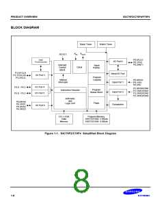
CLOCK CIRCUITS
System oscillation circuit generates the internal clock signals for the CPU and peripheral hardware.
The system clock can use a crystal, or ceramic oscillation source, or an externally-generated clock signal. To
drive S3C70F2/C70F4 using an external clock source, the external clock signal should be input to X , and its
in
inverted signal to X
out
.
4-bit power control register controls the oscillation on/off, and select the CPU clock. The internal system clock
signal (fx) can be divided internally to produce three CPU clock frequencies — fx/4, fx/8, or fx/64.
INTERRUPTS
Interrupt requests may be generated internally by on-chip processes (INTB, INTT0, and INTS) or externally by
peripheral devices (INT0 and INT1). There are two quasi-interrupts: INTK and INTW. INTK (KS0–KS2) detects
falling edges of incoming signals and INTW detects time intervals of 0.5 seconds or 3.91 milliseconds. The
following components support interrupt processing:
— Interrupt enable flags
— Interrupt request flags
— Interrupt priority registers
— Power-down termination circuit
1-5

 SAMSUNG [ SAMSUNG ]