PRODUCT OVERVIEW
S3C70F2/C70F4/P70F4
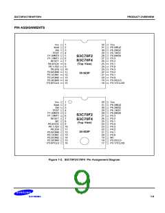
PIN DESCRIPTIONS
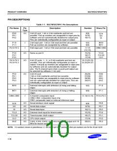
Table 1-1. S3C70F2/C70F4 Pin Descriptions
Description
Pin Name
Pin
Number
Share Pin
Type
P0.0
P0.1
P0.2
I/O
3-bit I/O port. 1-bit or 3-bit read/write and test are
possible. Pull-up resistors are assignable to input pins by
software and are automatically disabled for output pins.
Pins are individually configurable as input or output.
8(9)
9(10)
10(11)
SCK
SO
SI
P1.0
P1.1
I
I
2-bit input port. 1-bit or 2-bit read and test are possible.
Pull-up resistors are assignable by software.
5(5)
6(6)
INT0
INT1
P2.0–P2.3
4-bit input port. 1-bit or 4-bit read and test are possible.
11-14
CIN0–CIN3
(12-15)
P3.0
P3.1
P3.2
I/O
Same as port 0
15(16)
16(17)
17(18)
TCL0
TCLO0
CLO
P4.0–P4.3
P5.0–P5.3
I/O
I/O
4-bit I/O ports. 1-, 4-, or 8-bit read/write and test are
possible. Pins are individually configurable as input or
output. 4-bit pull-up resistors are assignable to input pins
by software and are automatically disabled for output
pins. The N-channel open-drain or push-pull output can
be selected by software (1-bit unit)
18-21(20-23)
22-25(24-27)
–
P6.0
P6.1
P6.2
P6.3
4-bit I/O port.
26(28)
27(29)
28(30)
29(31)
KS0
KS1
KS2
BUZ
1-bit or 4-bit read/write and test are possible.
Pull-up resistors are assignable to input pins by software
and are automatically disabled for output pins. Pins are
individually configurable as input or output.
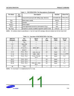
INT0
INT1
I
I
I
External interrupts with detection of rising and falling
edges
5(5)
6(6)
P1.0
P1.1
External interrupts with detection of rising or falling
edges
CIN0–CIN3
4-channel comparator input.
11-14(12-15)
P2.0–P2.3
CIN0–CIN2: comparator input only.
CIN3: comparator input or external reference input
I/O
Serial interface clock signal
P0.0
SCK
SO
8(9)
I/O
I/O
I/O
I/O
I/O
I/O
Serial data output
9(10)
P0.1
P0.2
P3.0
P3.1
P3.2
P6.3
SI
Serial data input
10(11)
15(16)
16(17)
17(18)
29(31)
TCL0
TCLO0
CLO
BUZ
External clock input for timer/counter
Timer/counter clock output
CPU clock output
2 kHz, 4 kHz, 8 kHz, or 16 kHz frequency output at 4.19
MHz for buzzer sound
NOTE: Pn numbers shown in parentheses '( )' are for 32-pin SOP package; other pin numbers are for the 30-pin SDIP.
1-10

 SAMSUNG [ SAMSUNG ]