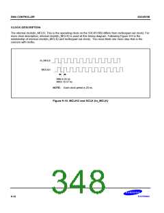
DMA CONTROLLER
S3C4510B
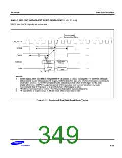
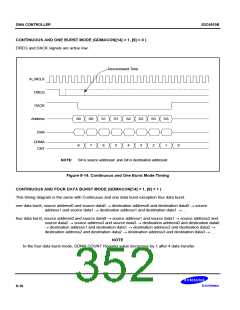
CONTINUOUS AND ONE BURST MODE (GDMACON[14] = 1, [9] = 0 )
DREQ and DACK signals are active low.
Recommand Time
In_MCLK
DREQ
DACK
Address
Data
S0
D0
S1
D1
S2
D2
S3
D3
GDMA
CNT
8
7
6
5
4
3
2
1
0
NOTE:
S# is source address#, and D# is destination address#.
Figure 9-14. Continuous and One Burst Mode Timing
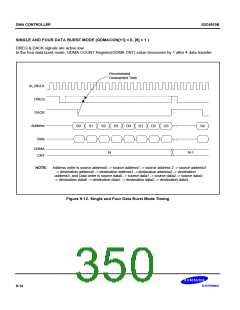
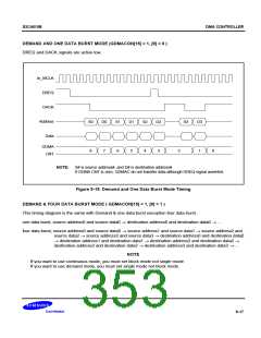
CONTINUOUS AND FOUR DATA BURST MODE (GDMACON[14] = 1, [9] = 1 )
This timing diagram is the same with Continuous and one data burst exception four data burst.
one data burst; source address0 and source data0 ® destination address0 and destination data0 ® source
address1 and source data1 ® destination address1 and destination data1 ® ...
four data burst; source address0 and source data0 ® source address1 and source data1 ® source address2 and
source data2 ® source address3 and source data3 ® destination address0 and destination data0
® destination address1 and destination data1 ® destination address2 and destination data2 ®
destination address2 and destination data2 ® destination address3 and destination data3 ® ...
NOTE
In the four data burst mode, GDMA COUNT Register value decreases by 1 after 4 data transfer.
9-16

 SAMSUNG [ SAMSUNG ]