S3C4510B
SYSTEM MANAGER
CONNECTION OF EXTERNAL MEMORY WITH VARIOUS DATA WIDTH
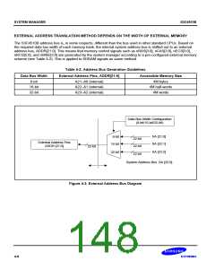
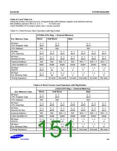
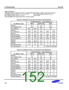
As another example, let us see how the S3C4510B maps CPU address spaces to physical addresses in external
memory:
When the CPU issues an arbitrary address to access an external memory device, the S3C4510B compares the
upper 10 bits of the issued address with the address pointers of all memory banks. It does this by consecutively
subtracting each address pointer value from the CPU address. There are two reasons why this subtraction
method is used:
·
To check the polarities of the subtraction result so as to identify which bank corresponds to the address
issued by the CPU.
·
To derive the offset address for the corresponding bank.
When the bank is identified and the offset has been derived, the corresponding bank selection signal (nRCS[5:0],
or nECS[3:0]) is generated, and the derived offset is driven to address external memory through the S3C4510B
physical address bus.
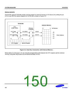
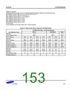
The S3C4510B can be configured as big-endian or little-endian mode by external little/big selection pin(LITTLE,
49).
In Big Endian mode, the most significant byte of the external memory data is stored at the lowest numbered byte
and the least significant byte at the highest numbered byte.
Eg.) In case of the external word memory system, Byte 0 of the memory is connected to data lines 31 through
24, D[31:24].
In Little Endian mode, vice versa.(See Figure 4-4 External Memory Interface)
4-7

 SAMSUNG [ SAMSUNG ]