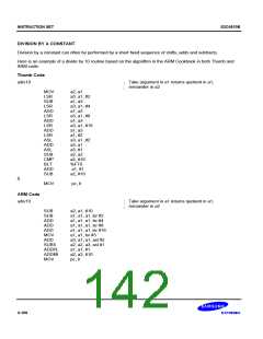
SYSTEM MANAGER
S3C4510B
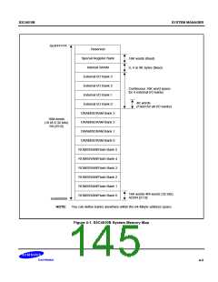
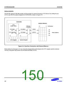
SYSTEM MEMORY MAP
Following are several important features to note about the S3C4510B system memory map:
·
·
·
The size and location of each memory bank is determined by the register settings for "current bank base
pointer" and "current bank end pointer". You can use this base/next bank pointer concept to set up a
consecutive memory map. To do this, you set the base pointer of the "next bank" to the same address as the
next pointer of the "current bank". Please note that when setting the bank control registers, the address
boundaries of consecutive banks must not overlap. This can be applied even if one or more banks are
disabled.
Four external I/O banks are defined in a continuous address space. A programmer can only set the base
pointer for external I/O bank 0. The start address of external I/O bank 1 is then calculated as the external I/O
bank 0 start address +16 K. Similarly, the start address for external I/O bank 2 is the external I/O bank 0 start
address + 32 K, and the start address for external I/O bank 3 is the external I/O bank 0 start address + 48 K.
Therefore, the total consecutive addressable space of the four external banks is defined as the start address
of external I/O bank 0 + 64 K bytes.
Within the addressable space, the start address of each I/O bank is not fixed. You can use bank control
registers to assign a specific bank start address by setting the bank's base pointer. The address resolution is
64 K bytes. The bank's start address is defined as "base pointer << 16" and the bank's end address (except
for external I/O banks) is "next pointer << 16 - 1".
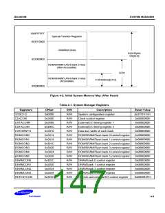
After a power-on or system reset, all bank address pointer registers are initialized to their default values. In this
case, all bank pointers except for the next pointer of ROM bank 0 are set to zero. This means that, except for
ROM bank 0, all banks are undefined following a system start-up.
The reset values for the next pointer and base pointer of ROM bank 0 are 0x200 and 0x000, respectively. This
means that a system reset automatically defines ROM bank 0 as a 32-Mbyte space with a start address of zero.
This initial definition of ROM bank 0 lets the system power-on or reset operation pass control to the user-supplied
boot code that is stored in external ROM. (This code is located at address 0 in the system memory map.) When
the boot code (i.e. ROM program) executes, it performs various system initialization tasks and reconfigures the
system memory map according to the application's actual external memory and device configuration.
The initial system memory map following system start-up is shown in Figure 4-2.
4-4

 SAMSUNG [ SAMSUNG ]