256MB, 512MB, 1GB Unbuffered DIMMs
DDR2 SDRAM
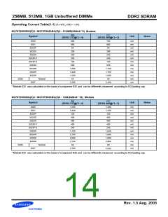
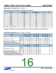
Operating Current Table(1-3) (TA=0oC, VDD= 1.9V)
M391T2953BG(Z)3 / M391T2953BG(Z)0 : 1GB(64Mx8 *18) ECC Module
D5
CC
Symbol
Unit
Notes
(DDR2-533@CL=4)
(DDR2-400@CL=3)
IDD0
IDD1
1,530
1,620
144
1,440
1,485
144
mA
mA
mA
mA
mA
mA
mA
mA
mA
mA
mA
mA
mA
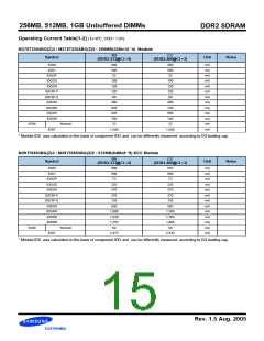
IDD2P
IDD2Q
IDD2N
IDD3P-F
IDD3P-S
IDD3N
IDD4W
IDD4R
IDD5B
450
450
540
540
540
540
270
270
1,260
2,430
2,250
2,385
99
1,170
1,890
1,890
2,250
99
IDD6
Normal
IDD7
3,105
3,015
* Module IDD was calculated on the basis of component IDD and can be differently measured according to DQ loading cap.
o
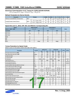
Input/Output Capacitance (VDD=1.8V, VDDQ=1.8V, TA=25 C)
Parameter
Min
Max
Min
Max
Min
Max
Symbol
Units
M378T2953BG(Z)3
M378T2953BG(Z)0
M378T6553BG(Z)3
M378T6553BG(Z)0
M378T3354BG(Z)3
M378T3354BG(Z)0
Non-ECC
CCK0
CCK1
CCK2
CI1
-
-
-
-
-
-
24
25
25
42
42
6
-
-
26
28
28
42
42
10
-
-
22
24
24
34
34
6
Input capacitance, CK and CK
pF
Input capacitance, CKE and CS
-
-
-
-
-
-
Input capacitance, Addr, RAS, CAS, WE
CI2
Input/output capacitance, DQ, DM, DQS, DQS CIO
M391T2953BG(Z)3
M391T2953BG(Z)0
M391T6553BG(Z)3
M391T6553BG(Z)0
ECC
Symbol
Units
CCK0
CCK1
CCK2
-
-
25
25
25
44
-
-
28
28
28
44
Input capacitance, CK and CK
pF
CI
Input capacitance, CKE and CS
-
-
-
-
-
-
1
CI
Input capacitance, Addr, RAS, CAS, WE
44
6
44
10
2
Input/output capacitance, DQ, DM, DQS, DQS CIO
* DM is internally loaded to match DQ and DQS identically.
Rev. 1.5 Aug. 2005
3-CD5/CC图片预览")
 SAMSUNG [ SAMSUNG ]