256MB, 512MB, 1GB Unbuffered DIMMs
DDR2 SDRAM
Operating Temperature Condition
Symbol
Parameter
Rating
Units
Notes
TOPER
Operating Temperature
0 to 95
°C
1, 2, 3
Note :
1. Operating Temperature is the case surface temperature on the center/top side of the DRAM. For the measurement conditions, please refer to JESD51.2
standard.
2. At 0 - 85 °C, operation temperature range are the temperature which all DRAM specification will be supported.
3. At 85 - 95 °C operation temperature range, doubling refresh commands in frequency to a 32ms period ( tREFI=3.9 us ) is required, and to enter to self
refresh mode at this temperature range, an EMRS command is required to change internal refresh rate.
Input DC Logic Level
Symbol
VIH(DC)
VIL(DC)
Parameter
Min.
VREF + 0.125
- 0.3
Max.
Units
Notes
Notes
DC input logic high
DC input logic low
VDDQ + 0.3
VREF - 0.125
V
V
Input AC Logic Level
Symbol
VIH(AC)
VIL(AC)
Parameter
Min.
Max.
Units
AC input logic high
AC input logic low
VREF + 0.250
-
-
V
V
VREF - 0.250
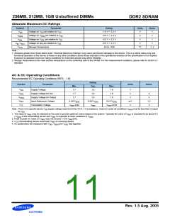
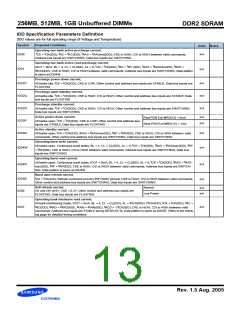
AC Input Test Conditions
Symbol
Condition
Value
Units
V
Notes
VREF
Input reference voltage
0.5 * V
1.0
1
1
DDQ
V
Input signal maximum peak to peak swing
Input signal minimum slew rate
V
SWING(MAX)
SLEW
1.0
V/ns
2, 3
Notes:
1. Input waveform timing is referenced to the input signal crossing through the V
(AC) level applied to the device under test.
IH/IL
2. The input signal minimum slew rate is to be maintained over the range from V
to V (AC) min for rising edges and the range from V
to V (AC)
REF IL
REF
IH
max for falling edges as shown in the below figure.
3. AC timings are referenced with input waveforms switching from V (AC) to V (AC) on the positive transitions and V (AC) to V (AC) on the negative
IL
IH
IH
IL
transitions.
V
V
V
V
V
V
V
DDQ
(AC) min
IH
(DC) min
IH
V
SWING(MAX)
REF
(DC) max
IL
IL
(AC) max
SS
delta TF
V
delta TR
Rising Slew =
- V (AC) max
IL
V
(AC) min - V
delta TR
REF
IH
REF
Falling Slew =
delta TF
< AC Input Test Signal Waveform >
Rev. 1.5 Aug. 2005
3-CD5/CC图片预览")
 SAMSUNG [ SAMSUNG ]