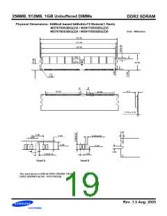
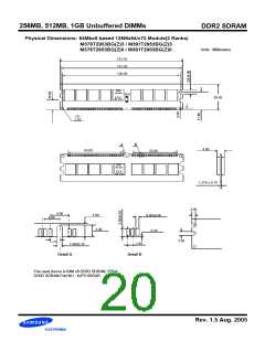
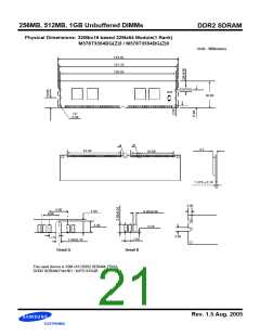
256MB, 512MB, 1GB Unbuffered DIMMs
DDR2 SDRAM
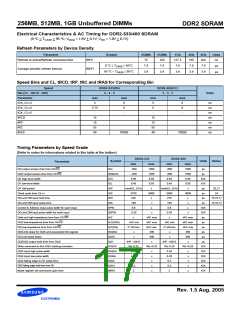
Electrical Characteristics & AC Timing for DDR2-533/400 SDRAM
(0 °C < T
< 95 °C; V
= 1.8V + 0.1V; V = 1.8V + 0.1V)
DDQ DD
CASE
Refresh Parameters by Device Density
Parameter
Symbol
256Mb
512Mb
1Gb
2Gb
4Gb
Units
Refresh to active/Refresh command time
tRFC
tREFI
75
105
127.5
195
tbd
ns
0 °C ≤ T
≤ 85°C
≤ 95°C
7.8
3.9
7.8
3.9
7.8
3.9
7.8
3.9
7.8
3.9
µs
µs
CASE
Average periodic refresh interval
85 °C < T
CASE
Speed Bins and CL, tRCD, tRP, tRC and tRAS for Corresponding Bin
Speed
DDR2-533(D5)
DDR2-400(CC)
3 - 3 - 3
Bin (CL - tRCD - tRP)
4 - 4 - 4
Units
Parameter
tCK, CL=3
tCK, CL=4
tCK, CL=5
tRCD
min
5
max
min
5
max
8
8
-
8
8
-
ns
ns
ns
ns
ns
ns
ns
3.75
-
5
-
15
15
55
40
15
15
55
40
tRP
tRC
tRAS
70000
70000
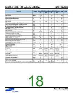
Timing Parameters by Speed Grade
(Refer to notes for informations related to this table at the bottom)
DDR2-533
min max
DDR2-400
min max
Symbol
Units
Notes
Parameter
DQ output access time from CK/CK
tAC
-500
-450
0.45
0.45
+500
-600
+600
ps
ps
DQS output access time from CK/CK
CK high-level width
tDQSCK
tCH
+450
-500
+500
0.55
0.45
0.55
tCK
tCK
ps
CK low-level width
tCL
0.55
0.45
0.55
CK half period
tHP
min(tCL, tCH)
x
min(tCL, tCH)
x
20,21
24
Clock cycle time, CL=x
tCK
3750
8000
5000
8000
ps
DQ and DM input hold time
tDH
225
x
275
x
ps
15,16,17
15,16,17
DQ and DM input setup time
tDS
100
x
150
x
ps
Control & Address input pulse width for each input
DQ and DM input pulse width for each input
Data-out high-impedance time from CK/CK
DQS low-impedance time from CK/CK
DQ low-impedance time from CK/CK
DQS-DQ skew for DQS and associated DQ signals
DQ hold skew factor
tIPW
0.6
x
0.6
x
tCK
tCK
ps
tDIPW
tHZ
0.35
x
0.35
x
x
tAC max
x
tAC max
tLZ(DQS)
tLZ(DQ)
tDQSQ
tQHS
tQH
tAC min
tAC max
tAC min
tAC max
ps
2* tACmin
tAC max
2* tACmin
tAC max
ps
x
300
x
350
ps
x
tHP - tQHS
WL-0.25
0.35
400
x
tHP - tQHS
WL-0.25
0.35
450
ps
DQ/DQS output hold time from DQS
Write command to first DQS latching transition
DQS input high pulse width
x
x
ps
tDQSS
tDQSH
tDQSL
tDSS
tDSH
tMRD
WL+0.25
WL+0.25
tCK
tCK
tCK
tCK
tCK
tCK
x
x
x
x
x
x
x
x
x
x
DQS input low pulse width
0.35
0.35
DQS falling edge to CK setup time
DQS falling edge hold time from CK
0.2
0.2
0.2
0.2
Mode register set command cycle time
2
2
Rev. 1.5 Aug. 2005
3-CD5/CC图片预览")
 SAMSUNG [ SAMSUNG ]