256MB, 512MB, 1GB Unbuffered DIMMs
DDR2 SDRAM
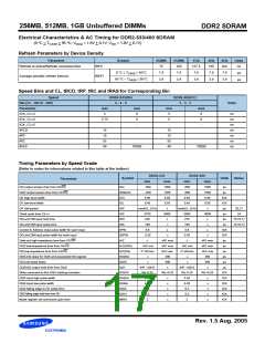
DDR2-533
DDR2-400
Symbol
Units
Notes
Parameter
min
max
0.6
x
min
max
0.6
x
Write postamble
Write preamble
tWPST
tWPRE
tIH
0.4
0.35
375
250
0.9
0.4
0.35
475
350
0.9
tCK
tCK
ps
Address and control input hold time
x
x
Address and control input setup time
Read preamble
tIS
x
x
ps
tRPRE
tRPST
tRRD
1.1
0.6
x
1.1
0.6
x
tCK
tCK
ns
Read postamble
0.4
0.4
Active to active command period for 1KB page size products
Active to active command period for 2KB page size products
Four Activate Window for 1KB page size products
Four Activate Window for 2KB page size products
CAS to CAS command delay
7.5
7.5
tRRD
tFAW
10
x
10
x
ns
37.5
50
37.5
50
ns
tFAW
ns
tCCD
tWR
2
2
tCK
ns
Write recovery time
15
x
x
x
15
x
x
x
Auto precharge write recovery + precharge time
Internal write to read command delay
Internal read to precharge command delay
Exit self refresh to a non-read command
Exit self refresh to a read command
tDAL
tWR+tRP
7.5
tWR+tRP
10
tCK
ns
tWTR
tRTP
7.5
7.5
ns
tXSNR
tXSRD
tXP
tRFC + 10
200
2
tRFC + 10
200
2
ns
tCK
tCK
tCK
tCK
Exit precharge power down to any non-read command
Exit active power down to read command
x
x
x
x
tXARD
tXARDS
2
2
Exit active power down to read command
(Slow exit, Lower power)
6 - AL
6 - AL
t
CKE minimum pulse width
(high and low pulse width)
tCK
3
3
CKE
t
ODT turn-on delay
2
2
2
2
tCK
ns
AOND
t
ODT turn-on
tAC(min)
tAC(max)+1
tAC(min)
tAC(max)+1
AON
t
ODT turn-on(Power-Down mode)
tAC(min)+2 2tCK+tAC(m tAC(min)+2
ax)+1
2tCK+tAC
(max)+1
ns
AONPD
t
ODT turn-off delay
ODT turn-off
2.5
2.5
2.5
2.5
tCK
ns
AOFD
t
tAC(min)
tAC(max)+ 0.6
tAC(max)+ 0.6
tAC(min)
AOF
2.5tCK+
2.5tCK+
t
ODT turn-off (Power-Down mode)
tAC(min)+2
tAC(min)+2
ns
AOFPD
tAC(max)+1
tAC(max)+1
ODT to power down entry latency
tANPD
tAXPD
tOIT
3
3
tCK
tCK
ns
ODT power down exit latency
8
8
OCD drive mode output delay
0
12
0
12
Minimum time clocks remains ON after CKE asynchronously drops LOW
tDelay
tIS+tCK +tIH
tIS+tCK +tIH
ns
Rev. 1.5 Aug. 2005
3-CD5/CC图片预览")
 SAMSUNG [ SAMSUNG ]