OneNAND512Mb(KFG1216U2B-xIB6)
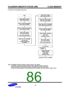
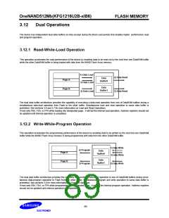
3.12 Dual Operations
FLASH MEMORY
The device has independent dual data buffers on-chip (except during the Boot Load period) that enables higher performance read
and program operation.
3.12.1 Read-While-Load Operation
This operation accelerates the read performance of the device by enabling data to be read out by the host from one DataRAM buffer
while the other DataRAM buffer is being loaded with data from the NAND Flash Array memory.
1) Data Load
2) Data Read
Data
Buffer0
Page A
3) Data Load
Data
Buffer1
Page B
2) Data Load
3) Data Read
The dual data buffer architecture provides the capability of executing a data-read operation from one of DataRAM buffers during a
simultaneous data-load operation from Flash to the other buffer. Simultaneous load and read operation to same data buffer is
prohibited. See sections 3.6 and 3.7 for more information on Load and Read Operations.
If host sets FBA, FSA, or FPA while loading into designated page, it will fail the internal load operation. Address registers should not
be updated until internal operation is completed.
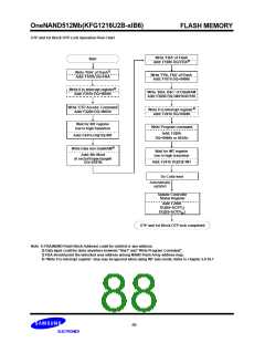
3.12.2 Write-While-Program Operation
This operation accelerates the programming performance of the device by enabling data to be written by the host into one DataRAM
buffer while the NAND Flash Array memory is being programmed with data from the other DataRAM buffer.
1) Data Write
2) Program
Data
Page A
Buffer0
3) Data Write
Data
Buffer1
Page B
3) Program
2) Data Write
The dual data buffer architecture provides the capability of executing a data-write operation to one of DataRAM buffers during simul-
taneous data-program operation to Flash from the other buffer. Simultaneous program and write operation to same data buffer is
prohibited. See sections 3.8 for more information on Program Operation.
If host sets FBA, FSA, or FPA while programming into designated page, it will fail the internal program operation. Address registers
should not be updated until internal operation is completed.
89

 SAMSUNG [ SAMSUNG ]