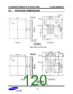
OneNAND512Mb(KFG1216U2B-xIB6)
7.2 Boot Sequence
FLASH MEMORY
One of the best features OneNAND has is that it can be a booting device itself since it contains an internally built-in boot loader
despite the fact that its core architecture is based on NAND Flash. Thus, OneNAND does not make any additional booting device
necessary for a system, which imposes extra cost or area overhead on the overall system.
As the system power is turned on, the boot code originally stored in NAND Flash Array is moved to BootRAM automatically and then
fetched by CPU through the same interface as SRAM’s or NOR Flash’s if the size of the boot code is less than 1KB. If its size is larger
than 1KB and less than or equal to 3KB, only 1KB of it can be moved to BootRAM automatically and fetched by CPU, and the rest of
it can be loaded into one of the DataRAMs whose size is 2KB by Load Command and CPU can take it from the DataRAM after finish-
ing the code-fetching job for BootRAM. If its size is larger than 3KB, the 1KB portion of it can be moved to BootRAM automatically
and fetched by CPU, and its remaining part can be moved to DRAM through two DataRAMs using dual buffering and taken by CPU
to reduce CPU fetch time.
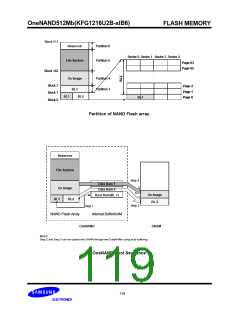
A typical boot scheme usually used to boot the system with OneNAND is explained at Partition of NAND Flash Array and OneNAND
Boot Sequence. In this boot scheme, boot code is comprised of BL1, where BL stands for Boot Loader, BL2, and BL3. Moreover, the
size of the boot code is larger than 3KB (the 3rd case above). BL1 is called primary boot loader in other words. Here is the table of
detailed explanations about the function of each boot loader in this specific boot scheme.
7.2.1
Boot Loaders in OneNAND
Boot Loaders in OneNAND
Boot Loader
BL1
Description
Moves BL2 from NAND Flash Array to DRAM through two DataRAMs using dual buffering
BL2
Moves OS image (or BL3 optionally) from NAND Flash Array to DRAM through two DataRams using dual buffering
Moves or writes the image through USB interface
BL3 (Optional)
NAND Flash Array of OneNAND is divided into the partitions as described at Partition of NAND Flash Array to show where each com-
ponent of code is located and how much portion of the overall NAND Flash Array each one occupies. In addition, the boot sequence
is listed below and depicted at Boot Sequence.
7.2.2
Boot Sequence
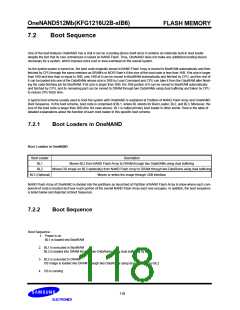
Boot Sequence :
1. Power is on
BL1 is loaded into BootRAM
2. BL1 is executed in BootRAM
BL2 is loaded into DRAM through two DataRams using dual buffering by BL1
3. BL2 is executed in DRAM
OS image is loaded into DRAM through two DataRams using dual buffering by BL2
4. OS is running
118

 SAMSUNG [ SAMSUNG ]